
Data Sheet


CC1101
SWRS061B Page 53 of 93
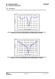
Component C
L
= 10 pF C
L
= 13 pF C
L
= 16 pF
C81 15 pF 22 pF 27 pF
C101 15 pF 22 pF 27 pF
Table 32: Crystal Oscillator Component Values
27.1 Reference Signal
The chip can alternatively be operated with a
reference signal from 26 to 27 MHz instead of
a crystal. This input clock can either be a full-
swing digital signal (0 V to VDD) or a sine
wave of maximum 1 V peak-peak amplitude.
The reference signal must be connected to the
XOSC_Q1 input. The sine wave must be
connected to XOSC_Q1 using a serial
capacitor. When using a full-swing digital
signal this capacitor can be omitted. The
XOSC_Q2 line must be left un-connected. C81
and C101 can be omitted when using a
reference signal.
28 External RF Match
The balanced RF input and output of
CC1101
share two common pins and are designed for
a simple, low-cost matching and balun network
on the printed circuit board. The receive- and
transmit switching at the
CC1101
front-end is
controlled by a dedicated on-chip function,
eliminating the need for an external RX/TX-
switch.
A few passive external components combined
with the internal RX/TX switch/termination
circuitry ensures match in both RX and TX
mode.
Although
CC1101
has a balanced RF
input/output, the chip can be connected to a
single-ended antenna with few external low
cost capacitors and inductors.
The passive matching/filtering network
connected to
CC1101
should have the following
differential impedance as seen from the RF-
port (RF_P and RF_N) towards the antenna:
Z
out 315 MHz
= 122 + j31 Ω
Z
out 433 MHz
= 116 + j41 Ω
Z
out 868/915 MHz
= 86.5 + j43 Ω
To ensure optimal matching of the
CC1101
differential output it is recommended to follow
the CC1101EM reference design ([5] or [6]) as
closely as possible. Gerber files for the
reference designs are available for download
from the TI website.
29 PCB Layout Recommendations
The top layer should be used for signal
routing, and the open areas should be filled
with metallization connected to ground using
several vias.
The area under the chip is used for grounding
and shall be connected to the bottom ground
plane with several vias. In the CC1101EM
reference designs ([5] and [6]) we have placed
5 vias inside the exposed die attached pad.
These vias should be “tented” (covered with
solder mask) on the component side of the
PCB to avoid migration of solder through the
vias during the solder reflow process.
The solder paste coverage should not be
100%. If it is, out gassing may occur during the
reflow process, which may cause defects
(splattering, solder balling). Using “tented” vias
reduces the solder paste coverage below
100%.
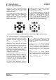
See Figure 28 for top solder resist and top
paste masks.
Each decoupling capacitor should be placed
as close as possible to the supply pin it is
supposed to decouple. Each decoupling
capacitor should be connected to the power
line (or power plane) by separate vias. The
best routing is from the power line (or power
plane) to the decoupling capacitor and then to
the
CC1101
supply pin. Supply power filtering is
very important.
Each decoupling capacitor ground pad should
be connected to the ground plane using a