
Data Sheet


CC1101
SWRS061B Page 52 of 93
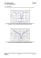
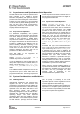
-20.0
-10.0
0.0
10.0
20.0
30.0
40.0
50.0
-3.00 -2.25 1.50 -1.00 -0.75 0.00 0.75 1.00 1.50 2.25 3.00
Frequency offset [MHz]
Selectivity [dB]
Figure 26: Typical Selectivity at 250 kBaud Data Rate, 868 MHz, GFSK, IF Frequency is 304kHz
and the Digital Channel Filter Bandwidth is 540 kHz
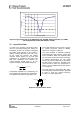
27 Crystal Oscillator
A crystal in the frequency range 26-27 MHz
must be connected between the XOSC_Q1
and XOSC_Q2 pins. The oscillator is designed
for parallel mode operation of the crystal. In
addition, loading capacitors (C81 and C101)
for the crystal are required. The loading
capacitor values depend on the total load
capacitance, C
L
, specified for the crystal. The
total load capacitance seen between the
crystal terminals should equal C
L
for the
crystal to oscillate at the specified frequency.
parasiticL
C
CC
C +
+
=
10181
11
1
The parasitic capacitance is constituted by pin
input capacitance and PCB stray capacitance.
Total parasitic capacitance is typically 2.5 pF.
The crystal oscillator circuit is shown in Figure
27. Typical component values for different
values of C
L
are given in Table 32.
The crystal oscillator is amplitude regulated.
This means that a high current is used to start
up the oscillations. When the amplitude builds
up, the current is reduced to what is necessary
to maintain approximately 0.4 Vpp signal
swing. This ensures a fast start-up, and keeps
the drive level to a minimum. The ESR of the
crystal should be within the specification in
order to ensure a reliable start-up (see Section
4.4 on page 13).
The initial tolerance, temperature drift, aging
and load pulling should be carefully specified
in order to meet the required frequency
accuracy in a certain application.
XOSC_Q1 XOSC_Q2
XTAL
C81 C101
Figure 27: Crystal Oscillator Circuit