
Data Sheet


CC1101
SWRS061B Page 45 of 93
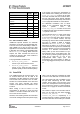
Description XOSC
Periods
26 MHz
Crystal
IDLE to RX, no calibration 2298 88.4µs
IDLE to RX, with calibration ~21037 809µs
IDLE to TX/FSTXON, no
calibration
2298 88.4µs
IDLE to TX/FSTXON, with
calibration
~21037 809µs
TX to RX switch 560 21.5µs
RX to TX switch 250 9.6µs
RX or TX to IDLE, no calibration 2 0.1µs
RX or TX to IDLE, with calibration ~18739 721µs
Manual calibration ~18739 721µs
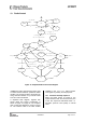
Table 28: State Transition Timing
19.7 RX Termination Timer
CC1101
has optional functions for automatic
termination of RX after a programmable time.
The main use for this functionality is wake-on-
radio (WOR), but it may be useful for other
applications. The termination timer starts when
in RX state. The timeout is programmable with
the MCSM2.RX_TIME setting. When the timer
expires, the radio controller will check the
condition for staying in RX; if the condition is
not met, RX will terminate.
The programmable conditions are:
• MCSM2.RX_TIME_QUAL=0: Continue
receive if sync word has been found
• MCSM2.RX_TIME_QUAL=1: Continue
receive if sync word has been found or
preamble quality is above threshold (PQT)
If the system can expect the transmission to
have started when enabling the receiver, the
MCSM2.RX_TIME_RSSI function can be used.
The radio controller will then terminate RX if
the first valid carrier sense sample indicates
no carrier (RSSI below threshold). See Section
17.4 on page 38 for details on Carrier Sense.
For ASK/OOK modulation, lack of carrier
sense is only considered valid after eight
symbol periods. Thus, the
MCSM2.RX_TIME_RSSI function can be used
in ASK/OOK mode when the distance between
“1” symbols is 8 or less.
If RX terminates due to no carrier sense when
the MCSM2.RX_TIME_RSSI function is used,
or if no sync word was found when using the
MCSM2.RX_TIME timeout function, the chip
will always go back to IDLE if WOR is disabled
and back to SLEEP if WOR is enabled.
Otherwise, the MCSM1.RXOFF_MODE setting
determines the state to go to when RX ends.
This means that the chip will not automatically
go back to SLEEP once a sync word has been
received. It is therefore recommended to
always wake up the microcontroller on sync
word detection when using WOR mode. This
can be done by selecting output signal 6 (see
Table 33 on page 55) on one of the
programmable GDO output pins, and
programming the microcontroller to wake up
on an edge-triggered interrupt from this GDO
pin.
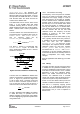
20 Data FIFO
The
CC1101
contains two 64 byte FIFOs, one
for received data and one for data to be
transmitted. The SPI interface is used to read
from the RX FIFO and write to the TX FIFO.
Section 10.5 contains details on the SPI FIFO
access. The FIFO controller will detect
overflow in the RX FIFO and underflow in the
TX FIFO.
When writing to the TX FIFO it is the
responsibility of the MCU to avoid TX FIFO
overflow. A TX FIFO overflow will result in an
error in the TX FIFO content.
Likewise, when reading the RX FIFO the MCU
must avoid reading the RX FIFO past its empty
value, since an RX FIFO underflow will result
in an error in the data read out of the RX FIFO.
The chip status byte that is available on the
SO pin while transferring the SPI header
contains the fill grade of the RX FIFO if the
access is a read operation and the fill grade of
the TX FIFO if the access is a write operation.
Section 10.1 on page 25 contains more details
on this.
The number of bytes in the RX FIFO and TX
FIFO can be read from the status registers
RXBYTES.NUM_RXBYTES and
TXBYTES.NUM_TXBYTES respectively. If a
received data byte is written to the RX FIFO at
the exact same time as the last byte in the RX