
Data Sheet
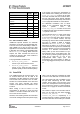


CC1101
SWRS061B Page 44 of 93
MCSM1.RXOFF_MODE will determine the
behaviour at the end of the received packet.
When the MCU has read the packet, it can put
the chip back into SLEEP with the SWOR strobe
from the IDLE state. The FIFO will loose its
contents in the SLEEP state.
The WOR timer has two events, Event 0 and
Event 1. In the SLEEP state with WOR
activated, reaching Event 0 will turn on the
digital regulator and start the crystal oscillator.
Event 1 follows Event 0 after a programmed
timeout.
The time between two consecutive Event 0 is
programmed with a mantissa value given by
WOREVT1.EVENT0 and WOREVT0.EVENT0,
and an exponent value set by
WORCTRL.WOR_RES. The equation is:
RESWOR
XOSC
Event
EVENT
f
t
_5
0
20
750
⋅
⋅⋅=
The Event 1 timeout is programmed with
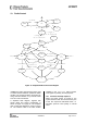
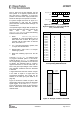
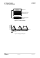
WORCTRL.EVENT1. Figure 19 shows the
timing relationship between Event 0 timeout
and Event 1 timeout.
Figure 19: Event 0 and Event 1 Relationship
The time from the
CC1101
enters SLEEP state
until the next Event0 is programmed to appear
(t
SLEEP
in Figure 19) should be larger than
11.08 ms when using a 26 MHz crystal and
10.67 ms when a 27 MHz crystal is used. If
t
SLEEP
is less than 11.08 (10.67) ms there is a
chance that the consecutive Event 0 will occur
128
750
⋅
XOSC
f
seconds
too early. Application Note AN047 [4] explains
in detail the theory of operation and the
different registers involved when using WOR,
as well as highlighting important aspects when
using WOR mode.
19.5.1 RC Oscillator and Timing
The frequency of the low-power RC oscillator
used for the WOR functionality varies with
temperature and supply voltage. In order to
keep the frequency as accurate as possible,
the RC oscillator will be calibrated whenever
possible, which is when the XOSC is running
and the chip is not in the SLEEP state. When
the power and XOSC is enabled, the clock
used by the WOR timer is a divided XOSC
clock. When the chip goes to the sleep state,
the RC oscillator will use the last valid
calibration result. The frequency of the RC
oscillator is locked to the main crystal
frequency divided by 750.
In applications where the radio wakes up very
often, typically several times every second, it
is possible to do the RC oscillator calibration
once and then turn off calibration
(WORCTRL.RC_CAL=0) to reduce the current
consumption. This requires that RC oscillator
calibration values are read from registers
RCCTRL0_STATUS and RCCTRL1_STATUS
and written back to RCCTRL0 and RCCTRL1
respectively. If the RC oscillator calibration is
turned off it will have to be manually turned on
again if temperature and supply voltage
changes.
Refer to Application Note AN047 [4] for further
details.
19.6 Timing
The radio controller controls most of the timing
in
CC1101
, such as synthesizer calibration, PLL
lock time, and RX/TX turnaround times. Timing
from IDLE to RX and IDLE to TX is constant,
dependent on the auto calibration setting.
RX/TX and TX/RX turnaround times are
constant. The calibration time is constant
18739 clock periods. Table 28 shows timing in
crystal clock cycles for key state transitions.
Power on time and XOSC start-up times are
variable, but within the limits stated in Table 7.
Note that in a frequency hopping spread
spectrum or a multi-channel protocol the
calibration time can be reduced from 721 µs to
approximately 150 µs. This is explained in
Section 32.2.