
Data Sheet

CC1101
SWRS061B Page 27 of 93
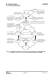
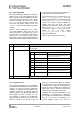
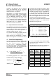
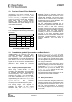
Figure 9 gives a brief overview of different
register access types possible.
10.6 PATABLE Access
The 0x3E address is used to access the
PATABLE, which is used for selecting PA
power control settings. The SPI expects up to
eight data bytes after receiving the address.
By programming the PATABLE, controlled PA
power ramp-up and ramp-down can be
achieved, as well as ASK modulation shaping
for reduced bandwidth. See SmartRF
®
Studio
[7] for recommended shaping / PA ramping
sequences.
See Section 24 on page 48 for details on
output power programming.
The PATABLE is an 8-byte table that defines
the PA control settings to use for each of the
eight PA power values (selected by the 3-bit
value FREND0.PA_POWER). The table is
written and read from the lowest setting (0) to
the highest (7), one byte at a time. An index
counter is used to control the access to the
table. This counter is incremented each time a
byte is read or written to the table, and set to
the lowest index when CSn is high. When the
highest value is reached the counter restarts
at zero.
The access to the PATABLE is either single
byte or burst access depending on the burst
bit. When using burst access the index counter
will count up; when reaching 7 the counter will
restart at 0. The R/W¯ bit controls whether the
access is a read or a write access.
If one byte is written to the PATABLE and this
value is to be read out then CSn must be set
high before the read access in order to set the
index counter back to zero.
Note that the content of the PATABLE is lost
when entering the SLEEP state, except for the
first byte (index 0).
Figure 9: Register Access Types
11 Microcontroller Interface and Pin Configuration
In a typical system,
CC1101
will interface to a
microcontroller. This microcontroller must be
able to:
• Program
CC1101
into different modes
• Read and write buffered data
• Read back status information via the 4-wire
SPI-bus configuration interface (SI, SO,
SCLK and CSn).
11.1 Configuration Interface
The microcontroller uses four I/O pins for the
SPI configuration interface (SI, SO, SCLK and
CSn). The SPI is described in Section 10 on
page 23.
11.2 General Control and Status Pins
The
CC1101
has two dedicated configurable
pins (GDO0 and GDO2) and one shared pin
(GDO1) that can output internal status
information useful for control software. These
pins can be used to generate interrupts on the
MCU. See Section 30 page 54 for more details
on the signals that can be programmed.
GDO1 is shared with the SO pin in the SPI
interface. The default setting for GDO1/SO is
3-state output. By selecting any other of the
programming options, the GDO1/SO pin will
become a generic pin. When CSn is low, the
pin will always function as a normal SO pin.
In the synchronous and asynchronous serial
modes, the GDO0 pin is used as a serial TX
data input pin while in transmit mode.
The GDO0 pin can also be used for an on-chip
analog temperature sensor. By measuring the