
Data Sheet

CC1101
SWRS061B Page 26 of 93
incremented by one each new byte (every 8
clock pulses). The burst access is either a
read or a write access and must be terminated
by setting CSn high.
For register addresses in the range 0x30-
0x3D, the burst bit is used to select between
status registers, burst bit is one, and command
strobes, burst bit is zero (see 10.4 below).
Because of this, burst access is not available
for status registers and they must be accesses
one at a time. The status registers can only be
read.
10.3 SPI Read
When reading register fields over the SPI
interface while the register fields are updated
by the radio hardware (e.g. MARCSTATE or
TXBYTES), there is a small, but finite,
probability that a single read from the register
is being corrupt. As an example, the
probability of any single read from TXBYTES
being corrupt, assuming the maximum data
rate is used, is approximately 80 ppm. Refer to
the
CC1101
Errata Notes [1] for more details.
10.4 Command Strobes
Command Strobes may be viewed as single
byte instructions to
CC1101
. By addressing a
command strobe register, internal sequences
will be started. These commands are used to
disable the crystal oscillator, enable receive
mode, enable wake-on-radio etc. The 13
command strobes are listed in Table 34 on
page 59.
The command strobe registers are accessed
by transferring a single header byte (no data is
being transferred). That is, only the R/W¯ bit,
the burst access bit (set to 0), and the six
address bits (in the range 0x30 through 0x3D)
are written. The R/W¯ bit can be either one or
zero and will determine how the
FIFO_BYTES_AVAILABLE field in the status
byte should be interpreted.
When writing command strobes, the status
byte is sent on the SO pin.
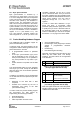
A command strobe may be followed by any
other SPI access without pulling CSn high.
However, if an SRES strobe is being issued,
one will have to waith for SO to go low again
before the next header byte can be issued as
shown in Figure 8. The command strobes are
executed immediately, with the exception of
the SPWD and the SXOFF strobes that are
executed when CSn goes high.
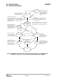
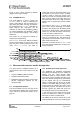
Figure 8: SRES Command Strobe
10.5 FIFO Access
The 64-byte TX FIFO and the 64-byte RX
FIFO are accessed through the 0x3F address.
When the R/W¯ bit is zero, the TX FIFO is
accessed, and the RX FIFO is accessed when
the R/W¯ bit is one.
The TX FIFO is write-only, while the RX FIFO
is read-only.
The burst bit is used to determine if the FIFO
access is a single byte access or a burst
access. The single byte access method
expects a header byte with the burst bit set to
zero and one data byte. After the data byte a
new header byte is expected; hence, CSn can
remain low. The burst access method expects
one header byte and then consecutive data
bytes until terminating the access by setting
CSn high.
The following header bytes access the FIFOs:
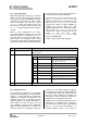
• 0x3F: Single byte access to TX FIFO
• 0x7F: Burst access to TX FIFO
• 0xBF: Single byte access to RX FIFO
• 0xFF: Burst access to RX FIFO
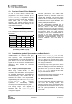
When writing to the TX FIFO, the status byte
(see Section 10.1) is output for each new data
byte on SO, as shown in Figure 7. This status
byte can be used to detect TX FIFO underflow
while writing data to the TX FIFO. Note that
the status byte contains the number of bytes
free before writing the byte in progress to the
TX FIFO. When the last byte that fits in the TX
FIFO is transmitted on SI, the status byte
received concurrently on SO will indicate that
one byte is free in the TX FIFO.
The TX FIFO may be flushed by issuing a
SFTX command strobe. Similarly, a SFRX
command strobe will flush the RX FIFO. A
SFTX or SFRX command strobe can only be
issued in the IDLE, TXFIFO_UNDERLOW, or
RXFIFO_OVERFLOW states. Both FIFOs are
flushed when going to the SLEEP state.