
Data Sheet

CC1101
SWRS061B Page 25 of 93
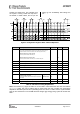
10.1 Chip Status Byte
When the header byte, data byte, or command
strobe is sent on the SPI interface, the chip
status byte is sent by the
CC1101
on the SO pin.
The status byte contains key status signals,
useful for the MCU. The first bit, s7, is the
CHIP_RDYn signal; this signal must go low
before the first positive edge of SCLK. The
CHIP_RDYn signal indicates that the crystal is
running.
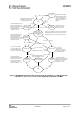
Bits 6, 5, and 4 comprise the STATE value.
This value reflects the state of the chip. The
XOSC and power to the digital core is on in
the IDLE state, but all other modules are in
power down. The frequency and channel
configuration should only be updated when the
chip is in this state. The RX state will be active
when the chip is in receive mode. Likewise, TX
is active when the chip is transmitting.
The last four bits (3:0) in the status byte con-
tains FIFO_BYTES_AVAILABLE. For read
operations (the R/W¯ bit in the header byte is
set to 1), the FIFO_BYTES_AVAILABLE field
contains the number of bytes available for
reading from the RX FIFO. For write
operations (the R/W¯ bit in the header byte is
set to 0), the FIFO_BYTES_AVAILABLE field
contains the number of bytes that can be
written to the TX FIFO. When
FIFO_BYTES_AVAILABLE=15, 15 or more
bytes are available/free.
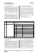
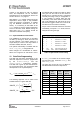
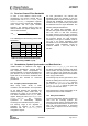
Table 17 gives a status byte summary.
Bits Name Description
7 CHIP_RDYn Stays high until power and crystal have stabilized. Should always be low when using
the SPI interface.
6:4 STATE[2:0] Indicates the current main state machine mode
Value State Description
000 IDLE IDLE state
(Also reported for some transitional states instead
of SETTLING or CALIBRATE)
001 RX Receive mode
010 TX Transmit mode
011 FSTXON Fast TX ready
100 CALIBRATE Frequency synthesizer calibration is running
101 SETTLING PLL is settling
110 RXFIFO_OVERFLOW RX FIFO has overflowed. Read out any
useful data, then flush the FIFO with SFRX
111 TXFIFO_UNDERFLOW TX FIFO has underflowed. Acknowledge with
SFTX
3:0 FIFO_BYTES_AVAILABLE[3:0] The number of bytes available in the RX FIFO or free bytes in the TX FIFO
Table 17: Status Byte Summary
10.2 Register Access
The configuration registers on the
CC1101
are
located on SPI addresses from 0x00 to 0x2E.
Table 35 on page 60 lists all configuration
registers. It is highly recommended to use
SmartRF
®
Studio [7] to generate optimum
register settings. The detailed description of
each register is found in Section 33.1 and
33.2, starting on page 63. All configuration
registers can be both written to and read. The
R/W¯ bit controls if the register should be
written to or read. When writing to registers,
the status byte is sent on the SO pin each time
a header byte or data byte is transmitted on
the SI pin. When reading from registers, the
status byte is sent on the SO pin each time a
header byte is transmitted on the SI pin.
Registers with consecutive addresses can be
accessed in an efficient way by setting the
burst bit (B) in the header byte. The address
bits (A
5
– A
0
) set the start address in an
internal address counter. This counter is