
Data Sheet

CC1101
SWRS061B Page 24 of 93
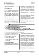
transfer the header byte. This indicates that
the crystal is running. Unless the chip was in
the SLEEP or XOFF states, the SO pin will
always go low immediately after taking CSn
low.
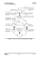
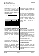
Figure 7: Configuration Registers Write and Read Operations
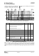
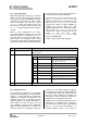
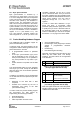
Parameter Description Min Max Units
SCLK frequency
100 ns delay inserted between address byte and data byte (single access), or
between address and data, and between each data byte (burst access).
- 10
SCLK frequency, single access
No delay between address and data byte
- 9
f
SCLK
SCLK frequency, burst access
No delay between address and data byte, or between data bytes
- 6.5
MHz
t
sp,pd
CSn low to positive edge on SCLK, in power-down mode 150 -
µs
t
sp
CSn low to positive edge on SCLK, in active mode 20 - ns
t
ch
Clock high 50 - ns
t
cl
Clock low 50 - ns
t
rise
Clock rise time - 5 ns
t
fall
Clock fall time - 5 ns
t
sd
Setup data (negative SCLK edge) to
positive edge on SCLK
(t
sd
applies between address and data bytes, and between
data bytes)
Single access
Burst access
55
76
-
-
ns
t
hd
Hold data after positive edge on SCLK 20 - ns
t
ns
Negative edge on SCLK to CSn high. 20 - ns
Table 16: SPI Interface Timing Requirements
Note: The minimum t
sp,pd
figure in Table 16 can be used in cases where the user does not read the
CHIP_RDYn signal. CSn low to positive edge on SCLK when the chip is woken from power-down
depends on the start-up time of the crystal being used. The 150 us in Table 16 is the crystal oscillator
start-up time measured on CC1101EM reference designs ([5] and [6]) using crystal AT-41CD2 from
NDK.