
Data Sheet

CC1101
SWRS061B Page 16 of 93
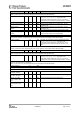
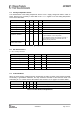
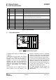
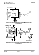
5 Pin Configuration
1
20 19 18 17 16
15
14
13
12
11
109876
5
4
3
2
GND
Exposed die
attach pad
SCLK
SO (GDO1)
GDO2
DVDD
DCOUPL
GDO0 (ATEST)
XOSC_Q1
AVDD
XOSC_Q2
AVDD
RF_P
RF_N
GND
AVDD
RBIAS
DGUARD
GND
SI
CSn
AVDD
Figure 1: Pinout Top View
Note: The exposed die attach pad must be connected to a solid ground plane as this is the main
ground connection for the chip.
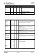
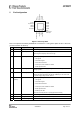
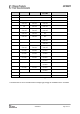
Pin # Pin Name Pin type Description
1 SCLK Digital Input Serial configuration interface, clock input
2 SO (GDO1) Digital Output Serial configuration interface, data output.
Optional general output pin when CSn is high
3 GDO2
Digital Output Digital output pin for general use:
• Test signals
• FIFO status signals
• Clear Channel Indicator
• Clock output, down-divided from XOSC
• Serial output RX data
4 DVDD Power (Digital) 1.8 - 3.6 V digital power supply for digital I/O’s and for the digital core
voltage regulator
5 DCOUPL Power (Digital) 1.6 - 2.0 V digital power supply output for decoupling.
NOTE: This pin is intended for use with the
CC1101
only. It can not be used
to provide supply voltage to other devices.
6 GDO0
(ATEST)
Digital I/O
Digital output pin for general use:
• Test signals
• FIFO status signals
• Clear Channel Indicator
• Clock output, down-divided from XOSC
• Serial output RX data
• Serial input TX data
Also used as analog test I/O for prototype/production testing
7 CSn Digital Input Serial configuration interface, chip select
8 XOSC_Q1 Analog I/O Crystal oscillator pin 1, or external clock input
9 AVDD Power (Analog) 1.8 - 3.6 V analog power supply connection