CC1101 CC1101 Low-Cost Low-Power Sub-1GHz RF Transceiver (Enhanced CC1100 ) Applications • Ultra low-power wireless applications operating in the 315/433/868/915 MHz ISM/SRD bands • Wireless alarm and security systems • Industrial monitoring and control • Wireless sensor networks • AMR – Automatic Meter Reading • Home and building automation Product Description The CC1101 is a low-cost sub- 1 GHz transceiver designed for very low-power wireless applications.
CC1101 Key Features • RF Performance • • • • • • High sensitivity (–111 dBm at 1.2 kBaud, 868 MHz, 1% packet error rate) Low current consumption (14.7 mA in RX, 1.2 kBaud, 868 MHz) Programmable output power up to +10 dBm for all supported frequencies Excellent receiver selectivity and blocking performance Programmable data rate from 1.
CC1101 Abbreviations Abbreviations used in this data sheet are described below.
CC1101 Table Of Contents APPLICATIONS .................................................................................................................................................. 1 PRODUCT DESCRIPTION................................................................................................................................ 1 KEY FEATURES .................................................................................................................................................
CC1101 15.4 15.5 15.6 16 16.1 16.2 16.3 17 17.1 17.2 17.3 17.4 17.5 17.6 18 18.1 18.2 19 19.1 19.2 19.3 19.4 19.5 19.6 19.7 20 21 22 22.1 23 24 25 26 27 27.1 28 29 30 31 31.1 31.2 32 32.1 32.2 32.3 32.4 32.5 32.6 32.7 32.8 32.9 32.10 PACKET HANDLING IN TRANSMIT MODE ................................................................................................... 33 PACKET HANDLING IN RECEIVE MODE .....................................................................................................
CC1101 33 33.1 33.2 33.3 34 34.1 34.2 34.3 34.4 34.5 35 36 37 37.1 37.2 38 39 CONFIGURATION REGISTERS........................................................................................................ 59 CONFIGURATION REGISTER DETAILS – REGISTERS WITH PRESERVED VALUES IN SLEEP STATE ............... 63 CONFIGURATION REGISTER DETAILS – REGISTERS THAT LOOSE PROGRAMMING IN SLEEP STATE ......... 83 STATUS REGISTER DETAILS......................................................................................
CC1101 1 Absolute Maximum Ratings Under no circumstances must the absolute maximum ratings given in Table 1 be violated. Stress exceeding one or more of the limiting values may cause permanent damage to the device. Caution! ESD sensitive device. Precaution should be used when handling the device in order to prevent permanent damage. Parameter Min Max Units Supply voltage –0.3 3.9 V Voltage on any digital pin –0.3 VDD + 0.3 V Condition All supply pins must have the same voltage max 3.
CC1101 4 Electrical Specifications 4.1 Current Consumption Tc = 25°C, VDD = 3.0V if nothing else stated. All measurement results are obtained using the CC1101EM reference designs ([5] and [6]). Reduced current settings (MDMCFG2.DEM_DCFILT_OFF=1) gives a slightly lower current consumption at the cost of a reduction in sensitivity. See for additional details on current consumption and sensitivity.
CC1101 Parameter Current consumption, 433MHz Current consumption, 868/915MHz Min Typ Max Unit Condition 16.0 mA Receive mode, 1.2 kBaud, reduced current, input at sensitivity limit 15.0 mA Receive mode, 1.2 kBaud, reduced current, input well above sensitivity limit 15.7 mA Receive mode, 38.4 kBaud , reduced current, input at sensitivity limit 15.0 mA Receive mode, 38.4 kBaud , reduced current, input well above sensitivity limit 17.
CC1101 4.2 RF Receive Section Tc = 25°C, VDD = 3.0V if nothing else stated. All measurement results are obtained using the CC1101EM reference designs ([5] and [6]). Parameter Digital channel filter bandwidth Min Typ 58 Max Unit Condition/Note 812 kHz User programmable. The bandwidth limits are proportional to crystal frequency (given values assume a 26.0 MHz crystal). 315 MHz, 1.2 kBaud data rate, sensitivity optimized, MDMCFG2.
CC1101 Parameter Min Typ Max Unit Condition/Note 868 MHz, 250 kBaud data rate, sensitivity optimized, MDMCFG2.DEM_DCFILT_OFF=0 (MSK, 1% packet error rate, 20 bytes packet length, 540 kHz digital channel filter bandwidth) Receiver sensitivity –94 dBm Sensitivity can be traded for current consumption by setting MDMCFG2.DEM_DCFILT_OFF=1. The typical current consumption is then reduced from 19.2 mA to 16.9 mA at sensitivity limit.
CC1101 Parameter Min Typ Max Unit Condition/Note -68 –57 dBm 25 MHz – 1 GHz (Maximum figure is the ETSI EN 300 220 limit) -66 –47 dBm Above 1 GHz (Maximum figure is the ETSI EN 300 220 limit) General Spurious emissions Typical radiated spurious emission is -49 dB measured at the VCO frequency. RX latency 9 bit Serial operation. Time from start of reception until data is available on the receiver data output pin is equal to 9 bit. Table 5: RF Receive Section 4.
CC1101 Parameter Min Typ Spurious emissions, conducted Harmonics not included Max Unit Condition/Note Measured with 10 dBm CW, TX frequency at 315.00 MHz, 433.00 MHz, 868.00 MHz or 915.00 MHz < -58 < -53 315 MHz dBm Frequencies below 960 MHz Frequencies above 960 MHz 433 MHz < -50 < -54 < -56 Frequencies below 1 GHz Frequencies above 1 GHz Frequencies within 47-74, 87.
CC1101 4.5 Low Power RC Oscillator Tc = 25°C, VDD = 3.0 V if nothing else is stated. All measurement results obtained using the CC1101EM reference designs ([5] and [6]). Parameter Min Typ Max Calibrated frequency 34.7 34.7 36 kHz ±1 % Frequency accuracy after calibration Temperature coefficient Supply voltage coefficient Initial calibration time Unit Condition/Note Calibrated RC Oscillator frequency is XTAL frequency divided by 750 +0.
CC1101 4.7 Analog Temperature Sensor The characteristics of the analog temperature sensor at 3.0 V supply voltage are listed in Table 10 below. Note that it is necessary to write 0xBF to the PTEST register to use the analog temperature sensor in the IDLE state. Parameter Min Typ Max Unit Output voltage at –40°C 0.651 V Output voltage at 0°C 0.747 V Output voltage at +40°C 0.847 V Output voltage at +80°C 0.945 V Temperature coefficient 2.
CC1101 GND RBIAS DGUARD GND Pin Configuration SI 5 20 19 18 17 16 SCLK 1 15 AVDD SO (GDO1) 2 14 AVDD GDO2 3 13 RF_N DVDD 4 12 RF_P DCOUPL 5 11 AVDD 7 8 9 10 GDO0 (ATEST) CSn XOSC_Q1 AVDD XOSC_Q2 6 GND Exposed die attach pad Figure 1: Pinout Top View Note: The exposed die attach pad must be connected to a solid ground plane as this is the main ground connection for the chip.
CC1101 Pin # Pin Name Pin type Description 10 XOSC_Q2 Analog I/O Crystal oscillator pin 2 11 AVDD Power (Analog) 1.8 -3.6 V analog power supply connection 12 RF_P RF I/O Positive RF input signal to LNA in receive mode Positive RF output signal from PA in transmit mode 13 RF_N RF I/O Negative RF input signal to LNA in receive mode Negative RF output signal from PA in transmit mode 14 AVDD Power (Analog) 1.8 - 3.6 V analog power supply connection 15 AVDD Power (Analog) 1.8 - 3.
CC1101 7 Application Circuit Only a few external components are required for using the CC1101. The recommended application circuits are shown in Figure 3 and Figure 4. The external components are described in Table 14, and typical values are given in Table 15. The balun and LC filter component values and their placement are important to keep the performance optimized. It is highly recommended to follow the CC1101EM reference design [5] and [6].
CC1101 1.8V-3.
CC1101 Component Value at 315MHz Value at 433MHz Value at 868/915MHz Manufacturer C51 100 nF ± 10%, 0402 X5R Murata GRM1555C series C81 27 pF ± 5%, 0402 NP0 Murata GRM1555C series C101 27 pF ± 5%, 0402 NP0 Murata GRM1555C series C121 6.8 pF ± 0.5 pF, 0402 NP0 3.9 pF ± 0.25 pF, 0402 NP0 1.0 pF ± 0.25 pF, 0402 NP0 Murata GRM1555C series C122 12 pF ± 5%, 0402 NP0 8.2 pF ± 0.5 pF, 0402 NP0 1.5 pF ± 0.25 pF, 0402 NP0 Murata GRM1555C series C123 6.8 pF ± 0.5 pF, 0402 NP0 5.6 pF ± 0.
CC1101 8 Configuration Overview CC1101 can be configured to achieve optimum • performance for many different applications. Configuration is done using the SPI interface.
CC1101 Sleep SPWD or wake-on-radio (WOR) SIDLE Default state when the radio is not receiving or transmitting. Typ. current consumption: 1.7 mA. CSn = 0 Lowest power mode. Most register values are retained. Current consumption typ 400 nA, or typ 900 nA when wake-on-radio (WOR) is enabled. IDLE SXOFF SCAL Used for calibrating frequency synthesizer upfront (entering CSn = 0 receive or transmit mode can Manual freq. then be done quicker). synth.
CC1101 9 Configuration Software CC1101 can be configured using the SmartRF® Studio software [7]. The SmartRF® Studio software is highly recommended for obtaining optimum register settings, and for evaluating performance and functionality. A screenshot of the SmartRF® Studio user interface for CC1101 is shown in Figure 6. After chip reset, all the registers have default values as shown in the tables in Section 33. The optimum register setting might differ from the default value.
CC1101 transfer the header byte. This indicates that the crystal is running. Unless the chip was in the SLEEP or XOFF states, the SO pin will always go low immediately after taking CSn low. Figure 7: Configuration Registers Write and Read Operations Parameter Description Min Max Units fSCLK SCLK frequency - 10 MHz - 9 - 6.5 100 ns delay inserted between address byte and data byte (single access), or between address and data, and between each data byte (burst access).
CC1101 10.1 Chip Status Byte When the header byte, data byte, or command strobe is sent on the SPI interface, the chip status byte is sent by the CC1101 on the SO pin. The status byte contains key status signals, useful for the MCU. The first bit, s7, is the CHIP_RDYn signal; this signal must go low before the first positive edge of SCLK. The CHIP_RDYn signal indicates that the crystal is running. Bits 6, 5, and 4 comprise the STATE value. This value reflects the state of the chip.
CC1101 incremented by one each new byte (every 8 clock pulses). The burst access is either a read or a write access and must be terminated by setting CSn high. For register addresses in the range 0x300x3D, the burst bit is used to select between status registers, burst bit is one, and command strobes, burst bit is zero (see 10.4 below). Because of this, burst access is not available for status registers and they must be accesses one at a time. The status registers can only be read. 10.
CC1101 Figure 9 gives a brief overview of different register access types possible. 10.6 PATABLE Access The 0x3E address is used to access the PATABLE, which is used for selecting PA power control settings. The SPI expects up to eight data bytes after receiving the address. By programming the PATABLE, controlled PA power ramp-up and ramp-down can be achieved, as well as ASK modulation shaping for reduced bandwidth. See SmartRF® Studio [7] for recommended shaping / PA ramping sequences.
CC1101 voltage on the GDO0 pin with an external ADC, the temperature can be calculated. Specifications for the temperature sensor are found in Section 4.7 on page 15. With default PTEST register setting (0x7F) the temperature sensor output is only available when the frequency synthesizer is enabled (e.g. the MANCAL, FSTXON, RX, and TX states). It is necessary to write 0xBF to the PTEST register to use the analog temperature sensor in the IDLE state.
CC1101 13 Receiver Channel Filter Bandwidth In order to meet different channel width requirements, the receiver channel filter is programmable. The MDMCFG4.CHANBW_E and MDMCFG4.CHANBW_M configuration registers control the receiver channel filter bandwidth, which scales with the crystal oscillator frequency.
CC1101 14.3 Byte Synchronization Byte synchronization is achieved by a continuous sync word search. The sync word is a 16 bit configurable field (can be repeated to get a 32 bit) that is automatically inserted at the start of the packet by the modulator in transmit mode. The demodulator uses this field to find the byte boundaries in the stream of bits.
CC1101 15.1 Data Whitening From a radio perspective, the ideal over the air data are random and DC free. This results in the smoothest power distribution over the occupied bandwidth. This also gives the regulation loops in the receiver uniform operation conditions (no data dependencies). Real world data often contain long sequences of zeros and ones. Performance can then be improved by whitening the data before transmitting, and de-whitening the data in the receiver.
CC1101 The preamble pattern is an alternating sequence of ones and zeros (10101010…). The minimum length of the preamble is programmable. When enabling TX, the modulator will start transmitting the preamble. When the programmed number of preamble bytes has been transmitted, the modulator will send the sync word and then data from the TX FIFO if data is available. If the TX FIFO is empty, the modulator will continue to send preamble bytes until the first byte is written to the TX FIFO.
CC1101 • Transmit at least 345 bytes (600 - 255), for example by filling the 64-byte TX FIFO six times (384 bytes transmitted). • Set PKTCTRL0.LENGTH_CONFIG=0. • The transmission ends when the packet counter reaches 88. A total of 600 bytes are transmitted. Internal byte counter in packet handler counts from 0 to 255 and then starts at 0 again 0,1,..........,88,....................255,0,........,88,..................,255,0,........,88,..................,255,0,.......................
CC1101 the optional address byte). If address recognition is enabled on the receiver, the second byte written to the TX FIFO must be the address byte. If fixed packet length is enabled, then the first byte written to the TX FIFO should be the address (if the receiver uses address recognition). The modulator will first send the programmed number of preamble bytes. If data is available in the TX FIFO, the modulator will send the two-byte (optionally 4-byte) sync word and then the payload in the TX FIFO.
CC1101 MISO line each time a header byte, data byte, or command strobe is sent on the SPI bus. It is recommended to employ an interrupt driven solution as high rate SPI polling will reduce the RX sensitivity. Furthermore, as explained in Section 10.3 and the CC1101 Errata Notes [1], when using SPI polling there 16 is a small, but finite, probability that a single read from registers PKTSTATUS , RXBYTES and TXBYTES is being corrupt. The same is the case when reading the chip status byte.
CC1101 17 Received Signal Qualifiers and Link Quality Information CC1101 has several qualifiers that can be used to increase the likelihood that a valid sync word is detected. 17.1 Sync Word Qualifier If sync word detection in RX is enabled in register MDMCFG2 the CC1101 will not start filling the RX FIFO and perform the packet filtering described in Section 15.3 before a valid sync word has been detected. The sync word qualifier mode is set by MDMCFG2.SYNC_MODE and is summarized in Table 24.
CC1101 Data rate [kBaud] RSSI_offset [dB], 433 MHz RSSI_offset [dB], 868 MHz 1.2 74 74 38.4 74 74 250 74 74 500 74 74 Table 25: Typical RSSI_offset Values 0 -10 -20 RSSI Readout [dBm] -30 -40 -50 -60 -70 -80 -90 -100 -110 -120 -120 -110 -100 -90 -80 -70 -60 -50 -40 -30 -20 -10 0 Input Power [dBm] 1.2 kBaud 38.4 kBaud 250 kBaud 500 kBaud Figure 13: Typical RSSI Value vs.
CC1101 Carrier Sense (CS) is used as a sync word qualifier and for CCA and can be asserted based on two conditions, which can be individually adjusted: • CS is asserted when the RSSI is above a programmable absolute threshold, and deasserted when RSSI is below the same threshold (with hysteresis). • CS is asserted when the RSSI has increased with a programmable number of dB from one RSSI sample to the next, and de-asserted when RSSI has decreased with the same number of dB.
CC1101 MAX_DVGA_GAIN value. This will reduce power consumption in the receiver front end, since the highest gain settings are avoided. command is sent on the SPI interface). This feature is called TX-if-CCA. Four CCA requirements can be programmed: 17.4.2 CS Relative Threshold • Always (CCA disabled, always goes to TX) The relative threshold detects sudden changes in the measured signal level.
CC1101 4 matrices. In the transmitter, the data bits from the rate ½ convolutional coder are written into the rows of the matrix, whereas the bit sequence to be transmitted is read from the columns of the matrix. Conversely, in the receiver, the received symbols are written into the columns of the matrix, whereas the data passed onto the convolutional decoder is read from the rows of the matrix. The convolutional coder is a rate 1/2 code with a constraint length of m = 4.
CC1101 19 Radio Control SIDLE SPWD | SWOR SLEEP 0 CAL_COMPLETE MANCAL 3,4,5 IDLE 1 CSn = 0 | WOR SXOFF SCAL CSn = 0 XOFF 2 SRX | STX | SFSTXON | WOR FS_WAKEUP 6,7 FS_AUTOCAL = 01 & SRX | STX | SFSTXON | WOR FS_AUTOCAL = 00 | 10 | 11 & SRX | STX | SFSTXON | WOR SETTLING 9,10,11 SFSTXON CALIBRATE 8 CAL_COMPLETE FSTXON 18 STX SRX STX TXOFF_MODE=01 SFSTXON | RXOFF_MODE = 01 STX | RXOFF_MODE = 10 TXOFF_MODE = 10 SRX | WOR RXTX_SETTLING 21 TX 19,20 SRX | TXOFF_MODE = 11 TX_UNDERFLOW 22
CC1101 After the automatic power-on reset or manual reset it is also recommended to change the signal that is output on the GDO0 pin. The default setting is to output a clock signal with a frequency of CLK_XOSC/192, but to optimize performance in TX and RX an alternative GDO setting should be selected from the settings found in Table 33 on page 55. • Pull CSn low and wait for SO to go low (CHIP_RDYn). • Issue the SRES strobe on the SI line.
CC1101 19.3 Voltage Regulator Control The voltage regulator to the digital core is controlled by the radio controller. When the chip enters the SLEEP state, which is the state with the lowest current consumption, the voltage regulator is disabled. This occurs after CSn is released when a SPWD command strobe has been sent on the SPI interface. The chip is now in the SLEEP state. Setting CSn low again will turn on the regulator and crystal oscillator and make the chip enter the IDLE state.
CC1101 MCSM1.RXOFF_MODE will determine the behaviour at the end of the received packet. When the MCU has read the packet, it can put the chip back into SLEEP with the SWOR strobe from the IDLE state. The FIFO will loose its contents in the SLEEP state. The WOR timer has two events, Event 0 and Event 1. In the SLEEP state with WOR activated, reaching Event 0 will turn on the digital regulator and start the crystal oscillator. Event 1 follows Event 0 after a programmed timeout.
CC1101 Description XOSC Periods 26 MHz Crystal IDLE to RX, no calibration 2298 88.4µs IDLE to RX, with calibration ~21037 809µs IDLE to TX/FSTXON, no calibration 2298 88.4µs IDLE to TX/FSTXON, with calibration ~21037 809µs TX to RX switch 560 21.5µs RX to TX switch 250 9.6µs RX or TX to IDLE, no calibration 2 0.1µs RX or TX to IDLE, with calibration ~18739 721µs Manual calibration ~18739 721µs Table 28: State Transition Timing 19.
CC1101 FIFO is read over the SPI interface, the RX FIFO pointer is not properly updated and the last read byte is duplicated. To avoid this problem one should never empty the RX FIFO before the last byte of the packet is received. For packet lengths less than 64 bytes it is recommended to wait until the complete packet has been received before reading it out of the RX FIFO. If the packet length is larger than 64 bytes the MCU must determine how many bytes can be read from the RX FIFO (RXBYTES.
CC1101 21 Frequency Programming The frequency programming in CC1101 is designed to minimize the programming needed in a channel-oriented system. To set up a system with channel numbers, the desired channel spacing is programmed with the MDMCFG0.CHANSPC_M and MDMCFG1.CHANSPC_E registers. The channel spacing registers are mantissa and exponent respectively. f carrier = ( ( The preferred IF frequency is programmed with the FSCTRL1.FREQ_IF register.
CC1101 23 Voltage Regulators CC1101 contains several on-chip linear voltage regulators, which generate the supply voltage needed by low-voltage modules. These voltage regulators are invisible to the user, and can be viewed as integral parts of the various modules. The user must however make sure that the absolute maximum ratings and required pin voltages in Table 1 and Table 13 are not exceeded. The voltage regulator for the digital core requires one external decoupling capacitor.
CC1101 315 MHz 433 MHz 868 MHz 915 MHz Output Power [dBm] Setting Current Consumption, Typ. [mA] Setting Current Consumption, Typ. [mA] Setting Current Consumption, Typ. [mA] Setting Current Consumption, Typ. [mA] -30 0x12 10.9 0x12 11.9 0x03 12.1 0x03 12.0 -20 0x0D 11.4 0x0E 12.4 0x0F 12.7 0x0E 12.6 -15 0x1C 12.0 0x1D 13.1 0x1E 13.4 0x1E 13.4 -10 0x34 13.5 0x34 14.4 0x27 15.0 0x27 14.9 -5 0x69 12.8 0x68 13.8 0x67 14.4 0x39 17.7 0 0x51 15.
CC1101 PATABLE(7)[7:0] The PA uses this setting. PATABLE(6)[7:0] PATABLE(5)[7:0] PATABLE(4)[7:0] Settings 0 to PA_POWER are used during ramp-up at start of transmission and ramp-down at end of transmission, and for ASK/OOK modulation. PATABLE(3)[7:0] PATABLE(2)[7:0] PATABLE(1)[7:0] PATABLE(0)[7:0] Index into PATABLE(7:0) The SmartRF® Studio software should be used to obtain optimum PATABLE settings for various output powers. e.
CC1101 26 Selectivity Figure 24 to Figure 26 show the typical selectivity performance (adjacent and alternate rejection). 50.0 40.0 Selectivity [dB] 30.0 20.0 10.0 0.0 -0.5 -0.4 -0.3 -0.2 -0.1 0.0 0.1 0.2 0.4 0.5 -10.0 -20.0 Frequency offset [MHz] Figure 24: Typical Selectivity at 1.2 kBaud Data Rate, 868 MHz, GFSK, 5.2 kHz Deviation. IF Frequency is 152.3 kHz and the Digital Channel Filter Bandwidth is 58 kHz 50.0 40.0 Selectivity [dB] 30.0 20.0 10.0 0.0 -1.0 -0.8 -0.5 -0.
CC1101 50.0 40.0 Selectivity [dB] 30.0 20.0 10.0 0.0 -3.00 -2.25 1.50 -1.00 -0.75 0.00 0.75 1.00 1.50 2.25 3.00 -10.0 -20.0 Frequency offset [MHz] Figure 26: Typical Selectivity at 250 kBaud Data Rate, 868 MHz, GFSK, IF Frequency is 304kHz and the Digital Channel Filter Bandwidth is 540 kHz 27 Crystal Oscillator A crystal in the frequency range 26-27 MHz must be connected between the XOSC_Q1 and XOSC_Q2 pins. The oscillator is designed for parallel mode operation of the crystal.
CC1101 Component CL = 10 pF CL = 13 pF CL = 16 pF C81 15 pF 22 pF 27 pF C101 15 pF 22 pF 27 pF Table 32: Crystal Oscillator Component Values 27.1 Reference Signal The chip can alternatively be operated with a reference signal from 26 to 27 MHz instead of a crystal. This input clock can either be a fullswing digital signal (0 V to VDD) or a sine wave of maximum 1 V peak-peak amplitude. The reference signal must be connected to the 28 XOSC_Q1 input.
CC1101 separate via. Direct connections between neighboring power pins will increase noise coupling and should be avoided unless absolutely necessary. The external components should ideally be as small as possible (0402 is recommended) and surface mount devices are highly recommended. Please note that components smaller than those specified may have differing characteristics. Precaution should be used when placing the microcontroller in order to avoid noise interfering with the RF circuitry.
CC1101 GDOx_CFG[5:0] 0 (0x00) 1 (0x01) 2 (0x02) 3 (0x03) 4 (0x04) 5 (0x05) 6 (0x06) 7 (0x07) 8 (0x08) 9 (0x09) 10 (0x0A) 11 (0x0B) 12 (0x0C) 13 (0x0D) 14 (0x0E) 15 (0x0F) 16 (0x10) 17 (0x11) 18 (0x12) 19 (0x13) 20 (0x14) 21 (0x15) 22 (0x16) 23 (0x17) 24 (0x18) 25 (0x19) 26 (0x1A) 27 (0x1B) 28 (0x1C) 29 (0x1D) 30 (0x1E) 31 (0x1F) 32 (0x20) 33 (0x21) 34 (0x22) 35 (0x23) 36 (0x24) 37 (0x25) 38 (0x26) 39 (0x27) 40 (0x28) 41 (0x29) 42 (0x2A) 43 (0x2B) 44 (0x2C) 45 (0x2D) 46 (0x2E) 47 (0x2F) 48 (0x30) 49 (0x31) 5
CC1101 31 Asynchronous and Synchronous Serial Operation Several features and modes of operation have been included in the CC1101 to provide backward compatibility with previous Chipcon products and other existing RF communication systems. For new systems, it is recommended to use the built-in packet handling features, as they can give more robust communication, significantly offload the microcontroller, and simplify software development. 31.
CC1101 32.2 Frequency Hopping Channel Systems and Multi- The 433 MHz, 868 MHz, or 915 MHz bands are shared by many systems both in industrial, office, and home environments. It is therefore recommended to use frequency hopping spread spectrum (FHSS) or a multi-channel protocol because the frequency diversity makes the system more robust with respect to interference from other systems operating in the same frequency band. FHSS also combats multipath fading.
CC1101 32.5 Continuous Transmissions 32.8 Low Cost Systems In data streaming applications the CC1101 opens up for continuous transmissions at 500 kBaud effective data rate. As the modulation is done with a closed loop PLL, there is no limitation in the length of a transmission (open loop modulation used in some transceivers often prevents this kind of continuous data streaming and reduces the effective data rate).
CC1101 33 Configuration Registers The configuration of CC1101 is done by programming 8-bit registers. The optimum configuration data based on selected system parameters are most easily found by using the SmartRF® Studio software [7]. Complete descriptions of the registers are given in the following tables. After chip reset, all the registers have default values as shown in the tables. The optimum register setting might differ from the default value.
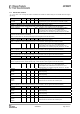
CC1101 Preserved in SLEEP State Details on Page Number Yes 63 Yes 63 Yes 63 Address Register Description 0x00 IOCFG2 0x01 IOCFG1 0x02 IOCFG0 GDO2 output pin configuration GDO1 output pin configuration GDO0 output pin configuration 0x03 FIFOTHR RX FIFO and TX FIFO thresholds Yes 64 0x04 SYNC1 Sync word, high byte Yes 64 0x05 SYNC0 Sync word, low byte Yes 64 0x06 PKTLEN Packet length Yes 65 0x07 PKTCTRL1 Packet automation control Yes 65 0x08 PKTCTRL0 Packet automat
CC1101 Address Register Description Details on page number 0x30 (0xF0) PARTNUM Part number for CC1101 84 0x31 (0xF1) VERSION Current version number 84 0x32 (0xF2) FREQEST Frequency Offset Estimate 84 0x33 (0xF3) LQI Demodulator estimate for Link Quality 84 0x34 (0xF4) RSSI Received signal strength indication 84 0x35 (0xF5) MARCSTATE Control state machine state 85 0x36 (0xF6) WORTIME1 High byte of WOR timer 85 0x37 (0xF7) WORTIME0 Low byte of WOR timer 85 0x38 (0xF8) PKTS
CC1101 Single Byte +0x80 IOCFG2 IOCFG1 IOCFG0 FIFOTHR SYNC1 SYNC0 PKTLEN PKTCTRL1 PKTCTRL0 ADDR CHANNR FSCTRL1 FSCTRL0 FREQ2 FREQ1 FREQ0 MDMCFG4 MDMCFG3 MDMCFG2 MDMCFG1 MDMCFG0 DEVIATN MCSM2 MCSM1 MCSM0 FOCCFG BSCFG AGCCTRL2 AGCCTRL1 AGCCTRL0 WOREVT1 WOREVT0 WORCTRL FREND1 FREND0 FSCAL3 FSCAL2 FSCAL1 FSCAL0 RCCTRL1 RCCTRL0 FSTEST PTEST AGCTEST TEST2 TEST1 TEST0 SRES SFSTXON SXOFF SCAL SRX STX SIDLE SRES SFSTXON SXOFF SCAL SRX STX SIDLE SWOR SPWD SFRX SFTX SWORRST SNOP PATABLE TX FIFO SWOR SPWD SFRX SFTX
CC1101 Table 37: SPI Address Space 33.1 Configuration Register Details – Registers with preserved values in SLEEP state 0x00: IOCFG2 – GDO2 Output Pin Configuration Bit Field Name Reset R/W Description 7 Reserved 6 GDO2_INV 0 R/W Invert output, i.e. select active low (1) / high (0) 5:0 GDO2_CFG[5:0] 41 (0x29) R/W Default is CHP_RDYn (See Table 33 on page 55).
CC1101 0x03: FIFOTHR – RX FIFO and TX FIFO Thresholds Bit Field Name Reset R/W Description 7:6 Reserved 0 R/W Write 0 for compatibility with possible future extensions 6 ADC_RETENTION 0 R/W 0: TEST1 = 0x31 and TEST2 = 0x88 when waking up from SLEEP 1: TEST1 = 0x35 and TEST2 = 0x81 when waking up from SLEEP 5:4 3:0 CLOSE_IN_RX [1:0] FIFO_THR[3:0] 0 (00) 7 (0111) R/W R/W For more details, please see DN010 [10] Setting RX Attenuation, Typical Values 0 (00) 0dB 1 (01) 6dB 2 (10) 12
CC1101 0x06: PKTLEN – Packet Length Bit Field Name Reset R/W Description 7:0 PACKET_LENGTH 255 (0xFF) R/W Indicates the packet length when fixed packet length mode is enabled. If variable packet length mode is used, this value indicates the maximum packet length allowed. 0x07: PKTCTRL1 – Packet Automation Control Bit Field Name Reset R/W Description 7:5 PQT[2:0] 0 (0x00) R/W Preamble quality estimator threshold.
CC1101 0x08: PKTCTRL0 – Packet Automation Control Bit Field Name 7 Reserved 6 WHITE_DATA Reset R/W Description R0 1 R/W Turn data whitening on / off 0: Whitening off 1: Whitening on 5:4 PKT_FORMAT[1:0] 0 (00) R/W 3 Reserved 0 R0 2 CRC_EN 1 R/W 1:0 LENGTH_CONFIG[1:0] 1 (01) R/W Format of RX and TX data Setting Packet format 0 (00) Normal mode, use FIFOs for RX and TX 1 (01) Synchronous serial mode, used for backwards compatibility.
CC1101 0x0B: FSCTRL1 – Frequency Synthesizer Control Bit Field Name 7:5 Reserved 4:0 FREQ_IF[4:0] Reset R/W Description R0 15 (0x0F) R/W The desired IF frequency to employ in RX. Subtracted from FS base frequency in RX and controls the digital complex mixer in the demodulator. f IF = f XOSC ⋅ FREQ _ IF 210 The default value gives an IF frequency of 381kHz, assuming a 26.0 MHz crystal.
CC1101 0x10: MDMCFG4 – Modem Configuration Bit Field Name Reset R/W 7:6 CHANBW_E[1:0] 2 (0x02) R/W 5:4 CHANBW_M[1:0] 0 (0x00) R/W Description Sets the decimation ratio for the delta-sigma ADC input stream and thus the channel bandwidth. BWchannel = f XOSC 8 ⋅ (4 + CHANBW _ M )·2 CHANBW _ E The default values give 203 kHz channel filter bandwidth, assuming a 26.0 MHz crystal.
CC1101 0x12: MDMCFG2 – Modem Configuration Bit Field Name Reset R/W Description 7 DEM_DCFILT_OFF 0 R/W Disable digital DC blocking filter before demodulator. 0 = Enable (better sensitivity) 1 = Disable (current optimized). Only for data rates ≤ 250 kBaud The recommended IF frequency changes when the DC blocking is disabled. Please use SmartRF® Studio [7] to calculate correct register setting.
CC1101 0x13: MDMCFG1– Modem Configuration Bit Field Name Reset R/W Description 7 FEC_EN 0 R/W Enable Forward Error Correction (FEC) with interleaving for packet payload 0 = Disable 1 = Enable (Only supported for fixed packet length mode, i.e. PKTCTRL0.
CC1101 0x15: DEVIATN – Modem Deviation Setting Bit Field Name 7 Reserved 6:4 DEVIATION_E[2:0] 3 Reserved 2:0 DEVIATION_M[2:0] Reset R/W Description R0 4 (0x04) R/W Deviation exponent R0 7 (111) R/W When MSK modulation is enabled: Sets fraction of symbol period used for phase change. Refer to the SmartRF® Studio software [7] for correct deviation setting when using MSK. When 2-FSK/GFSK modulation is enabled: Deviation mantissa, interpreted as a 4-bit value with MSB implicit 1.
CC1101 0x16: MCSM2 – Main Radio Control State Machine Configuration Bit Field Name Reset R/W Description 7:5 Reserved R0 Reserved 4 RX_TIME_RSSI 0 R/W Direct RX termination based on RSSI measurement (carrier sense). For ASK/OOK modulation, RX times out if there is no carrier sense in the first 8 symbol periods. 3 RX_TIME_QUAL 0 R/W When the RX_TIME timer expires, the chip checks if sync word is found when RX_TIME_QUAL=0, or either sync word is found or PQI is set when RX_TIME_QUAL=1.
CC1101 0x17: MCSM1– Main Radio Control State Machine Configuration Bit Field Name 7:6 Reserved 5:4 CCA_MODE[1:0] 3:2 RXOFF_MODE[1:0] Reset R/W Description R0 3 (11) 0 (00) R/W R/W Selects CCA_MODE; Reflected in CCA signal Setting Clear channel indication 0 (00) Always 1 (01) If RSSI below threshold 2 (10) Unless currently receiving a packet 3 (11) If RSSI below threshold unless currently receiving a packet Select what should happen when a packet has been received Setting Next state
CC1101 0x18: MCSM0– Main Radio Control State Machine Configuration Bit Field Name 7:6 Reserved 5:4 FS_AUTOCAL[1:0] Reset R/W Description R0 0 (00) R/W Automatically calibrate when going to RX or TX, or back to IDLE Setting When to perform automatic calibration 0 (00) Never (manually calibrate using SCAL strobe) 1 (01) When going from IDLE to RX or TX (or FSTXON) 2 (10) When going from RX or TX back to IDLE automatically 3 (11) Every 4 time when going from RX or TX to IDLE automatically
CC1101 0x19: FOCCFG – Frequency Offset Compensation Configuration Bit Field Name 7:6 Reserved 5 FOC_BS_CS_GATE 1 R/W If set, the demodulator freezes the frequency offset compensation and clock recovery feedback loops until the CS signal goes high. 4:3 FOC_PRE_K[1:0] 2 (10) R/W The frequency compensation loop gain to be used before a sync word is detected. 2 1:0 FOC_POST_K FOC_LIMIT[1:0] Reset R/W Description R0 1 2 (10) R/W R/W Setting Freq.
CC1101 0x1A: BSCFG – Bit Synchronization Configuration Bit Field Name Reset R/W Description 7:6 BS_PRE_KI[1:0] 1 (01) R/W The clock recovery feedback loop integral gain to be used before a sync word is detected (used to correct offsets in data rate): 5:4 3 2 1:0 BS_PRE_KP[1:0] BS_POST_KI BS_POST_KP BS_LIMIT[1:0] 2 (10) 1 1 0 (00) R/W R/W R/W R/W Setting Clock recovery loop integral gain before sync word 0 (00) KI 1 (01) 2KI 2 (10) 3KI 3 (11) 4KI The clock recovery feedbac
CC1101 0x1B: AGCCTRL2 – AGC Control Bit Field Name Reset R/W Description 7:6 MAX_DVGA_GAIN[1:0] 0 (00) R/W Reduces the maximum allowable DVGA gain.
CC1101 0x1C: AGCCTRL1 – AGC Control Bit Field Name 7 Reserved 6 AGC_LNA_PRIORITY 1 R/W Selects between two different strategies for LNA and LNA 2 gain adjustment. When 1, the LNA gain is decreased first. When 0, the LNA 2 gain is decreased to minimum before decreasing LNA gain.
CC1101 0x1D: AGCCTRL0 – AGC Control Bit Field Name Reset R/W Description 7:6 HYST_LEVEL[1:0] 2 (10) R/W Sets the level of hysteresis on the magnitude deviation (internal AGC signal that determine gain changes).
CC1101 0x1F: WOREVT0 –Low Byte Event0 Timeout Bit Field Name Reset R/W Description 7:0 EVENT0[7:0] 107 (0x6B) R/W Low byte of EVENT0 timeout register. The default EVENT0 value gives 1.0s timeout, assuming a 26.0 MHz crystal. 0x20: WORCTRL – Wake On Radio Control Bit Field Name Reset R/W Description 7 RC_PD 1 R/W Power down signal to RC oscillator. When written to 0, automatic initial calibration will be performed 6:4 EVENT1[2:0] 7 (111) R/W Timeout setting from register block.
CC1101 0x21: FREND1 – Front End RX Configuration Bit Field Name Reset R/W Description 7:6 LNA_CURRENT[1:0] 1 (01) R/W Adjusts front-end LNA PTAT current output 5:4 LNA2MIX_CURRENT[1:0] 1 (01) R/W Adjusts front-end PTAT outputs 3:2 LODIV_BUF_CURRENT_RX[1:0] 1 (01) R/W Adjusts current in RX LO buffer (LO input to mixer) 1:0 MIX_CURRENT[1:0] 2 (10) R/W Adjusts current in mixer 0x22: FREND0 – Front End TX Configuration Bit Field Name Reset 7:6 Reserved 5:4 LODIV_BUF_CURRENT_TX[1:0
CC1101 0x24: FSCAL2 – Frequency Synthesizer Calibration Bit Field Name Reset R/W Description 7:6 Reserved 5 VCO_CORE_H_EN 0 R/W Choose high (1) / low (0) VCO 4:0 FSCAL2[4:0] 10 (0x0A) R/W Frequency synthesizer calibration result register. VCO current calibration result and override value Fast frequency hopping without calibration for each hop can be done by calibrating upfront for each frequency and saving the resulting FSCAL3, FSCAL2 and FSCAL1 register values.
CC1101 33.2 Configuration Register Details – Registers that Loose Programming in SLEEP State 0x29: FSTEST – Frequency Synthesizer Calibration Control Bit Field Name Reset R/W Description 7:0 FSTEST[7:0] 89 (0x59) R/W For test only. Do not write to this register. 0x2A: PTEST – Production Test Bit Field Name Reset R/W Description 7:0 PTEST[7:0] 127 (0x7F) R/W Writing 0xBF to this register makes the on-chip temperature sensor available in the IDLE state.
CC1101 33.3 Status Register Details 0x30 (0xF0): PARTNUM – Chip ID Bit Field Name Reset R/W Description 7:0 PARTNUM[7:0] 0 (0x00) R Chip part number 0x31 (0xF1): VERSION – Chip ID Bit Field Name Reset R/W Description 7:0 VERSION[7:0] 4 (0x04) R Chip version number. 0x32 (0xF2): FREQEST – Frequency Offset Estimate from Demodulator Bit Field Name Reset 7:0 FREQOFF_EST R/W Description R The estimated frequency offset (2’s complement) of the carrier. Resolution is 14 FXTAL/2 (1.
CC1101 0x35 (0xF5): MARCSTATE – Main Radio Control State Machine State Bit Field Name Reset R/W 7:5 Reserved R0 4:0 MARC_STATE[4:0] R Description Main Radio Control FSM State Value State name State (Figure 16, page 41) 0 (0x00) SLEEP SLEEP 1 (0x01) IDLE IDLE 2 (0x02) XOFF XOFF 3 (0x03) VCOON_MC MANCAL 4 (0x04) REGON_MC MANCAL 5 (0x05) MANCAL MANCAL 6 (0x06) VCOON FS_WAKEUP 7 (0x07) REGON FS_WAKEUP 8 (0x08) STARTCAL CALIBRATE 9 (0x09) BWBOOST SETTLING 10 (0x0A) FS
CC1101 0x38 (0xF8): PKTSTATUS – Current GDOx Status and Packet Status Bit Field Name 7 Reset R/W Description CRC_OK R The last CRC comparison matched. Cleared when entering/restarting RX mode. 6 CS R Carrier sense 5 PQT_REACHED R Preamble Quality reached 4 CCA R Channel is clear 3 SFD R Sync word found 2 GDO2 R Current GDO2 value. Note: the reading gives the non-inverted value irrespective of what IOCFG2.GDO2_INV is programmed to.
CC1101 0x3D (0xFC): RCCTRL0_STATUS – Last RC Oscillator Calibration Result Bit Field Name Reset R/W 7 Reserved R0 6:0 RCCTRL0_STATUS[6:0] R Description Contains the value from the last run of the RC oscillator calibration routine. For usage description refer to Aplication Note AN047 [4]. 34 Package Description (QLP 20) All dimensions are in millimetres, angles in degrees. NOTE: The CC1101 is available in RoHS lead-free package only.
CC1101 34.1 Recommended PCB Layout for Package (QLP 20) Figure 31: Recommended PCB Layout for QLP 20 Package Note: Figure 31 is an illustration only and not to scale. There are five 10 mil via holes distributed symmetrically in the ground pad under the package. See also the CC1101EM reference designs ([5] and [6]). 34.2 Package Thermal Properties Thermal Resistance Air velocity [m/s] 0 Rth,j-a [K/W] 40.4 Table 39: Thermal Properties of QLP 20 Package 34.
CC1101 34.5 Carrier Tape and Reel Specification Carrier tape and reel is in accordance with EIA Specification 481.
CC1101 36 References [1] CC1101 Errata Notes (swrz020.pdf) [2] AN001 SRD Regulations for Licence Free Transceiver Operation (swra090.pdf) [3] AN039 Using the CC1100 in the European 433 and 868 MHz ISM Bands (swra054.pdf) [4] AN047 CC1100/CC2500 – Wake-On-Radio (swra126.pdf) [5] CC1101EM 315 - 433 MHz Reference Design 1.0 (swrr043.zip) [6] CC1101EM 868 – 915 MHz Reference Design 2.0 (swrr044.zip) [7] SmartRF® Studio (swrc046.zip) [8] CC1100 CC2500 Examples Libraries (swrc021.
CC1101 37 General Information 37.1 Document History Revision Date Description/Changes SWRS061B 2007.06.05 Changed name on DN009 Close-in Reception with CC1101 to DN010 Close-in Reception with CC1101. Added info regarding how to reduce spurious emission at 699 MHz.
CC1101 38 Address Information Texas Instruments Norway AS Gaustadalléen 21 N-0349 Oslo NORWAY Tel: +47 22 95 85 44 Fax: +47 22 95 85 46 Web site: http://www.ti.com/lpw 39 TI Worldwide Technical Support Internet TI Semiconductor Product Information Center Home Page: TI Semiconductor KnowledgeBase Home Page: support.ti.com support.ti.com/sc/knowledgebase Product Information Centers Americas +1(972) 644-5580 +1(972) 927-6377 support.ti.com/sc/pic/americas.
CC1101 Asia Phone Fax Email Internet International Domestic Australia China Hong Kong India Indonesia Korea Malaysia New Zealand Philippines Singapore Taiwan Thailand +886-2-23786800 Toll-Free Number 1-800-999-084 800-820-8682 800-96-5941 +91-80-51381665 (Toll) 001-803-8861-1006 080-551-2804 1-800-80-3973 0800-446-934 1-800-765-7404 800-886-1028 0800-006800 001-800-886-0010 +886-2-2378-6808 tiasia@ti.com or ti-china@ti.com support.ti.com/sc/pic/asia.
IMPORTANT NOTICE Texas Instruments Incorporated and its subsidiaries (TI) reserve the right to make corrections, modifications, enhancements, improvements, and other changes to its products and services at any time and to discontinue any product or service without notice. Customers should obtain the latest relevant information before placing orders and should verify that such information is current and complete.