
Specifications


18 The X.21 Interface
The X.21 Interface
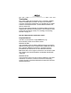
A pin-out diagram for the X.21
interface is shown in Figure 7.
The signal definitions and names
are listed in Table 6.
Figure 7. X.21 Interface
PGND
T(A)
C(A)
R(A)
I(A)
S(A)
B(A)
SGND
T(B)
C(B)
R(B)
I(B)
S(B)
B(B)
1
10
19
Table 6. X.21 Interface Signals
Pin # Signal Name Direction CCITT #
1 PGND Protective Ground Common 101
7 SGND Signal Ground Common 102
9 S(A) Signal Element Timing (+) Input 115A
10 S(B) Signal Element Timing (-) Input 115B
11 R(A) Receive Data (+) Input 104A
12 R(B) Receive Data (-) Input 104B
13 I(B) Indication (-) Input 109B
14 B(A) Byte Timing (+) Input 114A
16 I(A) Indication (+) Input 109A
19 T(A) Transmit Data (+) Output 103A
20 C(B) Control Signal (-) Output 105B
23 B(B) Byte Timing (-) Input 114B
24 C(A) Control Signal (+) Output 105A
26 T(B) Transmit Data (-) Output 103B