
User manual


Selecting an Interface Cable 137
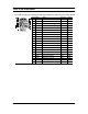
The EIA-530 Interface
The EIA-530 interface pin-out diagram and signal definitions and names are shown
below.
Pin # Signal Name Direction CCITT # EIA
1 PGND Protective Ground Common 101 -
2 TXD+ Transmit Data Output 103A BA(A)
3 RXD+ Receive Data Input 104A BB(A)
4 RTS+ Request to Send Output 105A CA(A)
5 CTS+ Clear to Send Input 106A CB(A)
6 DSR+ Data Set Ready Input 107A CC(A)
7 SGND Signal Ground Common 102B AB
8 DCD+ Data Carrier Detect Input 109A CF(A)
9 RTXC- Receive Clock (DCE) Input 115B DD(B)
10 DCD- Data Carrier Detect Input 109B CF(B)
11 CLK- Transmit Clock (DTE) Output 113B DA(B)
12 TRXC- Transmit Clock (DCE) Input 114B DB(B)
13 CTS- Clear to Send Output 106B CB(B)
14 TXD- Transmit Data Output 103B BA(B)
15 TRXC+ Transmit Clock (DCE) Input 114A DB(A)
16 RXD- Receive Data Input 104B BB(B)
17 RTXC+ Receive Clock (DCE) Input 115A DD(A)
18 TEST Local Loopback Activation Output 141A LL
19 RTS- Request to Send Output 105B CA(B)
20 DTR+ Data Terminal Ready Output 108A CD(A)
21 RLB Remote Loopback Output 140A RL
22 DSR- Data Set Ready Input 107B CC(B)
23 DTR- Data Terminal Ready Output 108B CD(B)
24 CLK+ Transmit Clock (DTE) Output 113A DA(A)
25 TI Test Indicator Input 142A TM
PGND
RXD+
RTS+
1
RI
DCD+
GND
TXD+
TRXC+
RTXC+
CTS+
DSR+
DTR+
CLK+
RXD-
RTS-
DCD-
TXD-
TRXC-
RTXC-
CTS-
DSR-
DTR-
TEST
RLB
TI
CLK-
37
19
20