
Datasheet

Datasheet
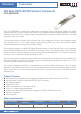
Transceiver
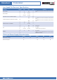
Pin Descriptions
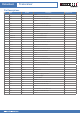
Pin Logic Symbol Description Plug Sequence
4
39 GND Ground
1
1A
40 CML-I Tx6n Transmitter Inverted Data Input 3A
41 CML-I Tx6p Transmitter Non-Inverted Data Input 3A
42 GND Ground
1
1A
43 CML-I Tx8n Transmitter Inverted Data Input 3A
44 CML-I Tx8p Transmitter Non-Inverted Data Input 3A
45 GND Ground
1
1A
46 Reserved For future use 3A
47 VS1 Module Vendor Specific
3
3A
48 VccRx1 3.3V Power Suppl
y2A
49 VS2 Module Vendor Specific
2
3A
50 VS3 Module Vendor Specific
3
3A
51 GND Ground
1
1A
52 CML-O Rx7p Receiver Non-Inverted Data Output 3A
53 CML-O Rx7n Receiver Inverted Data Output 3A
54 GND Ground
1
1A
55 CML-O Rx5p Receiver Non-Inverted Data Output 3A
56 CML-O Rx5n Receiver Inverted Data Output 3A
57 GND Ground
1
1A
58 GND Ground
1
1A
59 CML-O Rx6n Receiver Inverted Data Output 3A
60 CML-O Rx6p Receiver Non-Inverted Data Output 3A
61 GND Ground
1
1A
62 CML-O Rx8n Receiver Inverted Data Output 3A
63 CML-O Rx8p Receiver Non-Inverted Data Output 3A
64 GND Ground
1
1A
65 NC No Connect 3A
66 Reserved For future use 3A
67 VccTx1 3.3 V Power Suppl
y2A
68 Vcc2 3.3 V Power Suppl
y2A
69 LVTTL-I ePPS Precision Time Protocol (PTP) reference clock input 3A
70 GND Ground
1
1A
71 CML-I Tx7p Transmitter Non-Inverted Data Input 3A
72 CML-I Tx7n Transmitter Inverted Data Input 3A
73 GND Ground
1
1A
74 CML-I Tx5p Transmitter Non-Inverted Data Input 3A
75 CML-I Tx5n Transmitter Inverted Data Input 3A
76 GND Ground
1
1A
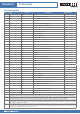
Note 1. QSFP-DD uses common ground (GND) for all signals and supply (power). All are common within the QSFP-DD module and all module
voltages are referenced to this potential unless otherwise noted. Connect these directly to the host board signal-common ground plane.
Note 2. VccRx, VccRx1, Vcc1, Vcc2, VccTx and VccTx1 shall be applied concurrently. VccRx, VccRx1, Vcc1, Vcc2, VccTx and VccTx1 may be internally
connected within the module in any combination. The connector Vcc pins are each rated for a maximum current of 1000 mA.
Note 3. All Vendor Specific, Reserved, No Connect and ePPS (if not used) pins may be terminated with 50 Ohms to ground on the host. Pad 65 (No
Connect) shall be leſt unconnected within the module. Vendor specific and Reserved pads shall have an impedance to GND that is greater
than 10 kOhms and less than 100 pF.
Note 4. Plug Sequence specifies the mating sequence of the host connector and module. The sequence is 1A, 2A, 3A, 1B, 2B, 3B. (see page 4
for pad locations) Contact sequence A will make, then break contact with additional QSFP-DD pads. Sequence 1A, 1B will then occur
simultaneously, followed by 2A, 2B, followed by 3A, 3B.