
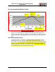
User Manual

Red
pine Signals, Inc. Proprietary and confidential Page 16
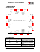
RS9110
-
N
-
11
-
02
802.11bgn
WLAN
Module
Data Sheet
Version
1.48
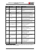
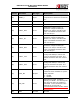
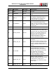
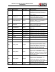
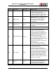
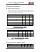
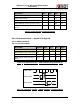
Pin No. Pin Name Pin Type Description
The pin should be left grounded
ex
c
ept as describe in mode (iii) as
described in note below for Sleep
Clock Input.
36)
U
ART2_IN Inout
UART-2 input. This is a firmware
configured GPIO pin. Where not
used, it should be left open.
37) V
OUTBCKDC1P3 Power
Internal DC-DC convertor output. A
Schottky diode is to be placed on
this line for protection.
38) F
BDC1P3 Power
Feedback for the DC-DC Converter
Input to the LDO’s. This has to be
connected to FBDC1P3.
39) V
INLDOP123 Power
Input to the LDO’s. Connect this to
FBDC1P3.
40) N
C No-connect This pin is to be left unconnected
41) N
C No-connect This pin is to be left unconnected
42) N
C No-connect This pin is to be left unconnected
43) V
RF33 Power 3.3 Volts input to the RF transceiver
44) V
RF33 Power 3.3 Volts input to the RF transceiver
45) G
ND Ground Ground
46) P
SPI_CSN1 Output
When enabled as a SPI interface
pin, this is the chip-select output
from SPI Master. This is a firmware
configured GPIO pin. Where not
used, it should be left open. Default
firmware does not use this pin
47) P
SPI_MISO Input
When enabled as a SPI interface
pin, this is the SPI Master data
input. This is a firmware configured
GPIO pin. Where not used, it should
be left open. Default firmware does
not use this pin.
48) P
SPI_MOSI Output
When enabled as a SPI interface
pin, this is the SPI Master data
output. This is a firmware
configured GPIO pin. Where not
used, it should be left open. Default
firmware does not use this pin.
49) P
SPI_CLK Output
When enabled as a SPI interface