
User Manual

Red
pine Signals, Inc. Proprietary and confidential Page 14
RS9110
-
N
-
11
-
02
802.11bgn
WLAN
Module
Data Sheet
Version
1.48
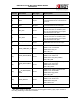
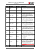
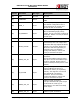
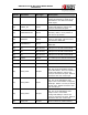
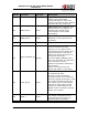
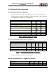
Pin No. Pin Name Pin Type Description
15)
R
ESET_n Input
Power-on reset. Active low, and
required to be active for at least 20
ms
16)
G
ND Ground Ground
17)
D
VDD33 Power 3.3 Volts Input to the I/O Rail
18) U
ART1_OUT Inout
UART Port1 output. This is a
firmware configured GPIO pin.
Where not used, it should be left
open. The default firmware does
not use this pin.
19) U
ART1_IN Inout
UART Port1 input. This is a
firmware configured GPIO pin.
Where not used, it should be left
open. The default firmware does
not use this pin.
20) U
ART2_OUT Inout
UART Port2 output. This is a
firmware configured GPIO pin.
Where not used, it should be left
open. The default firmware does
not use this pin.
21) U
ART1_CTS Inout
UART Port1 CTS. This is a firmware
configured GPIO pin. Where not
used, it should be left open. The
default firmware does not use this
pin.
22) U
ART1_RTS Inout
UART Port1 RTS. This is a firmware
configured GPIO pin. Where not
used, it should be left open. The
default firmware does not use this
pin.
23) X
TAL_EN Output
This signal controls an external
reference clock oscillator for power-
save purposes.
1 – Enable
0 – Disable
24) L
ED_ON Inout
LED Control signal. Indicates
activity on WLAN – the device pulls
this line low when the module is
activated. To be connected to the
Cathode of an LED with a
recommended series resistor of 820
ohms to VDD.
25) G
ND Ground Ground