
Data Sheet
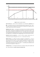
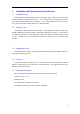
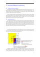
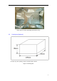
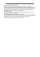
Table Of Contents

15
8. Layout and Soldering Considerations
8.1
Soldering Recommendations
FSC-BT816S is compatible with industrial standard reflow profile for Pb-free solders. The
reflow profile used is dependent on the thermal mass of the entire populated PCB, heat
transfer efficiency of the oven and particular type of solder paste used. Consult the datasheet
of particular solder paste for profile configurations.
Feasycom will give following recommendations for soldering the module to ensure reliable
solder joint and operation of the module after soldering. Since the profile used is process and
layout dependent, the optimum profile should be studied case by case. Thus following
recommendation should be taken as a starting point guide.
8.2 Layout Guidelines
It is strongly recommended to use good layout practices to ensure proper operation of the
module. Placing copper or any metal near antenna deteriorates its operation by having effect
on the matching properties. Metal shield around the antenna will prevent the radiation and thus
metal case should not be used with the module. Use grounding vias separated max 3 mm
apart at the edge of grounding areas to prevent RF penetrating inside the PCB and causing an
unintentional resonator. Use GND vias all around the PCB edges.
The mother board should have no bare conductors or vias in this restricted area, because
it is not covered by stop mask print. Also no copper (planes, traces or vias) are allowed in this
area, because of mismatching the on-board antenna.
Figure 7: FSC-BT816S Restricted Area
Following recommendations helps to avoid EMC problems arising in the design. Note that
each design is unique and the following list do not consider all basic design rules such as
avoiding capacitive coupling between signal lines. Following list is aimed to avoid EMC