Bluetooth Module Data Sheet Document Type: SA-20 Document Version: V1.1 Release Date: November 12.
Release Record Version Number Revision 1.
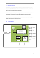
1. INTRODUCTION FSC-BT816S is a fully integrated Bluetooth module that complies with Bluetooth 4.2 dual mode protocols(BR/EDR/LE). It provides several interfaces such as UART, I2C, PCM, AIO, PIO, etc,which can customized different applications. FSC-BT816S supports various profiles. It integrates MCU, Baseband controller, RF, etc. in a small package, so the designers can have better flexibilities for the product shapes. FSC-BT816S can be controlled by UART port or other interfaces.
1.2 Feature ◆ Fully qualified Bluetooth 4.2/3.0/2.1/2.0/1.2/1.1 ◆ Postage stamp sized form factor. ◆ Low power. ◆ Class 1.5 support(high output power). ◆ The default UART Baud rate is 115.2Kbps and can support from 1200bps up to 921Kbps,. ◆ UART, I2C , PCM/I2S data connection interfaces. ◆ Embedded Bluetooth stack profiles support(requires no host stack): SPP, HID, and all LE protocols. 1.
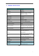
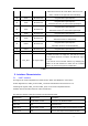
2. GENERAL SPECIFICATION General Specification Chipset CC2564C Product ID SMQSA-20 13mm(W) x 26.9mm(L) x 2.0mm(H) Dimension (Tolerance: ±0.2mm) Bluetooth Specification Bluetooth V4.2 (Dual Mode) Power Supply 3.3 Volt DC Output Power 5.06 dBm Sensitivity -90dBm@0.1%BER Frequency Band 2.402GHz -2.480GHz ISM band Modulation FHSS,GFSK,DPSK,DQPSK Baseband Crystal OSC 26MHz 1600hops/sec, 1MHz channel space,79 Hopping & channels Channels(BT 4.
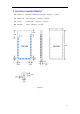
3. PHYSICAL CHARACTERISTIC Dimension: 13mm(W) x 26.9mm(L) x 2.0mm(H) Tolerance: ±0.2mm Module size: 13mm X 26.9mm Tolerance: ±0.2mm Pad size: 1mmX0.8mm Pad pitch: 1.5mm Tolerance: ±0.1mm Tolerance: ±0.
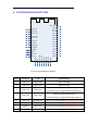
4. PIN DEFINITION DESCRIPTIONS 1 2 UART_TX UART_RX 3 UART_CTS 4 5 UART_RTS PCM_CLK 6 PCM_OUT 7 EXT_ANT GND PIO11 PIO10 PIO9 PIO8 PIO7 `` 36 35 34 33 32 31 30 27 9 Tran/AIO0 PIO3 26 10 Disc/AIO1 PIO2 25 11 RESET PIO1 24 12 VDD_3V3 PIO0 23 13 GND GND 22 GND PIO4 PIO12 PIO13 PIO14 PCM_SYNC SWDIO 8 NC SWCLK 29 28 BOOT0 PCM_IN PIO6 PIO5 14 15 16 17 18 19 20 21 Figure 4: FSC-BT816S PIN Diagram Pin NO.
Alternative Function 1: Analogue programmable I/O line. Alternative Function 2: Host MCU change UART 9 Tran/AIO0 I/O transmission mode. When bluetooth connection established, H = instruction mode L = throughput mode Alternative Function 1: Analogue programmable I/O line. 10 Disc/AIO1 I/O Alternative Function 2: Host MCU disconnect bluetooth. When bluetooth connection established, a rising edge of the PIN will cause disconnection with remote device. Reset if low.
Alternative Function: BT Power Mode, low level in run mode, it will be set to high level when fall asleep.
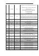
Table 3 Possible UART Settings Property Possible Values BCSP-Specific Hardware Enable or Disable Baud Rate 1200bps to 921Kbps Flow Control RTS/CTS or None Data bit length 8bits Parity None, Odd or Even Number of Stop Bits 1 or 2 Table 4 Default Data Format Property Possible Values Baud Rate 115.2Kbps Flow Control None Data bit length 8bit Parity None Number of Stop Bits 1 Table 5 5.2 PCM CODEC Interface The PCM signal level 1.8V. 6. 7. 8. 9. 10. 11. 12. 13. 14.
5.2.1 PCM Master Symbol Parameter Tclk Cycle time Condition Min Max 244.14 15625(64kHZ) Unit (4.296MHZ) Tw High or low pulse width 50% of Tclk min Tis PCM-IN setup time 25 Tih PCM-IN hold time 0 Top PCM-OUT propagation time 40pF load 0 10 Top PCM-SYNC propagation time 40pF load Table 6 0 10 Condition Min Max ns 5.2.2 PCM Slave Symbol Parameter Tclk Cycle time 62.
Analog to Digital Converter (ADC) The ADC is a Successive Approximation Register (SAR) architecture, with a resolution of up to 12 bits at up to one million samples per second. The integrated input max can select inputs from 4 external pins and 6 internal signals. 6. RECOMMENDED TEMPERATURE REFLOW PROFILE Prior to any reflow, it is important to ensure the modules were packaged to prevent moisture absorption.
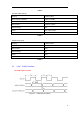
℃ 250 217 210 A 25 0 B 1 2 C 3 D 4 E 5 6 Figure 6: Typical Lead-free Re-flow Pre-heat zone (A) — This zone raises the temperature at a controlled rate, typically 0.5 – 2 °C/s. The purpose of this zone is to preheat the PCB board and components to 120 ~ 150 °C. This stage is required to distribute the heat uniformly to the PCB board and completely remove solvent to reduce the heat shock to components.
7. Reliability and Environmental Specification 7.1 Temperature test Put the module in demo board which uses exit power supply, power on the module and connect to mobile. Then put the demo in the ‐40℃ space for 1 hour and then move to +85℃ space within 1minute, after 1 hour move back to ‐40℃ space within1 minute. This is 1 cycle. The cycles are 32 times and the units have to pass the testing. 7.2 Vibration Test The module is being tested without package. The displacement requests 1.
8. Layout and Soldering Considerations 8.1 Soldering Recommendations FSC-BT816S is compatible with industrial standard reflow profile for Pb-free solders. The reflow profile used is dependent on the thermal mass of the entire populated PCB, heat transfer efficiency of the oven and particular type of solder paste used. Consult the datasheet of particular solder paste for profile configurations.
problems caused by RF part of the module. Use good consideration to avoid problems arising from digital signals in the design. Ensure that signal lines have return paths as short as possible. For example if a signal goes to an inner layer through a via, always use ground vias around it. Locate them tightly and symmetrically around the signal vias. Routing of any sensitive signals should be done in the inner layers of the PCB. Sensitive traces should have a ground area above and under the line.
Figure 8,9,10: Product Packaging Information (Tray) 9.
Integration instructions for host product manufacturers according to KDB 996369 D03 OEM Manual v01 2.2 List of applicable FCC rules FCC Part 15 Subpart C 15.247 & 15.209 . 2.3 Specific operational use conditions The module can be used for mobile applications with a maximum 2dBi antenna.
2.10 Additional testing, Part 15 Subpart B disclaimer The modular transmitter is only FCC authorized for FCC Part 15 Subpart C 15.247 & 15.209 and that the host product manufacturer is responsible for compliance to any other FCC rules that apply to the host not covered by the modular transmitter grant of certification.
Validity of using the module certification: In the event that these conditions cannot be met (for example certain laptop configurations or co-location with another transmitter), then the FCC authorization for this module in combination with the host equipment is no longer considered valid and the FCC ID of the module cannot be used on the final product.