
User Manual


As C
leak,SIGNAL
increases, a larger current flows during V
gate
transitions, and more common-
mode RF current couples onto the network twisted pair. This common-mode RF current can
generate EMI in the 30-500 MHz frequency range, well in excess of CFR Part 15 Subpart B
or CISPR 22 Class B levels, even when the capacitance of C
leak,SIGNAL
from a clock line to
Earth ground is less than 1 pF. Thus, it is essential to guard clock lines (and keep them on
the top side of the PCB, if possible) for meeting Subpart B limits.
By using 0.1 μF or 0.01 μF decoupling capacitors at each digital IC power pin, you can reduce
V
DD33
and logic ground noise. You can then use logic ground as a ground shield for other
noisy digital signals and clock lines.
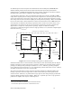
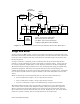
In addition, some amount of filtering might also be required on a Series 6000 device's power
supply input, depending on the level of noise generated by the application circuitry. A good
way to achieve this filtering is to place ferrite chokes in series with the power input traces
adjacent to the power connector. Figure 32 shows a typical power supply circuit illustrating
the placement of these ferrite chokes.
IN
GND
OUT
Local
Power
Connector
Input
3-Terminal Voltage Regulator
+
+3.3 V Output
Figure 32. Power Supply Input Filtering Using Ferrite Chokes
Testing for EMI to comply with the CISPR 22 Radio Disturbance Characteristics test
standard takes two forms:
• Radiated EMI testing checks for RF noise that radiates from network and power
cables (or from inside the device)
• Conducted EMI testing checks for RF noise that radiates from the power supply
connection to the AC mains
Compliance with the CISPR 22 Class A standard is required for industrial products, and
compliance with the Class B standard is required for products that can be used in residential
environments.
The following general rules and guidelines summarize EMI design considerations:
• The faster the system clock speed for a Series 6000 device, the higher the level of
EMI.
• Better V
DD3
decoupling quiets RF noise at the sources (the digital ICs), which lowers
radiated EMI.
• A four-layer PCB generates less EMI than a two-layer PCB because the extra layers
provide better V
DD3
decoupling and more effective logic ground guarding.
Radiated and Conducted Immunity
The EN 61000-4-3 RF Susceptibility and EN 61000-4-6 Conducted RF Immunity tests ensure
that a device’s operation is not impaired by strong electromagnetic fields, such as those
generated near cellular phones and portable radios.
82 Design and Test for Electromagnetic Compatibility