
User Manual


FT 6000
Smart Transceiver
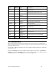
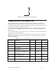
U
1
FT 5000
SVC~
1
IO
0
2
IO1
3
IO2
4
IO
3
5
VDD1V8
6
IO4
7
VDD3V3
8
IO5
9
IO6
10
IO7
11
IO8
12
IO
9
13
IO10
14
IO11
15
VDD1V8
16
TRST~
17
VDD3V3
18
TCK
19
TMS
20
TDI
21
TDO
22
XIN
23
XOUT
24
VDDPLL
25
GNDPLL
26
VOUT1V8
27
RST~
28
VIN3V3
29
VDD3V3
30
AVDD
3V
3
31
NETN
32
AGND
33
NETP
34
NC
35
GND
36
TXON
37
RXON
38
CP4
39
CS0~
40
VDD3V3
41
VDD3V3
42
SDA_CS1~
43
VDD1V
8
44
SCL
45
MISO
46
SCK
47
MOSI
48
GND
49
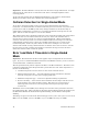
Figure 12. Connections for the Ground Pins
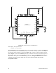
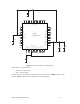
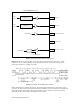
Connect the VDDPLL pin (25) to the VOUT1V8 pin (27), with an associated chip ferrite
bead, as shown in Figure 13. Connect the GNDPLL pin (26) to GND, with an associated
chip ferrite bead. In addition, add stabilizing capacitors across the VDDPLL and GNDPLL
pins. Place each capacitor directly adjacent to the PLL pins, on the top layer of the PCB.
C1
0.01 uF
12
C2
0.1 uF
12
L1
BEAD
1 2
L2
BEAD
1 2
GNDPLL
VDDPLL VOUT1V8
Figure 13. Connections for the PLL Pins
In the figure, the capacitors are:
• C1: 0.01 µF Ceramic
• C2: 0.1 µF Ceramic
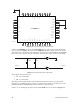
The chip ferrite beads should be rated for ≥50 mA saturation current, provide ≥120 Ω
impedance at 100 MHz per 20 ºC, and have a DC resistance ≤1 Ω. An example part is the
Laird Technologies
®
LI0603E151R-10 part (formerly a Steward part).
Connect a 1 to 10 kΩ pull-up resistor to the JTAG TCK pin (19), as shown in Figure 14.
42 Hardware Resources