
User Manual


Pin Assignments
Although the pin assignments for the Neuron 6000 Processor and the FT 6000 Smart
Transceiver are very similar, there are a few differences, as described in the following
sections.
All pins can withstand 2 kV Electrostatic Discharge (ESD) voltage, as tested according to
MIL-STD-883 Method 3015.7.
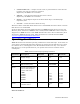
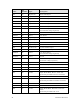
FT 6000 Smart Transceiver
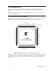
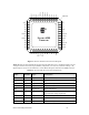
Figure 8 shows the pinout for the FT 6000 Smart Transceiver. The central rectangle in the
figure represents the bottom pad (pin 49), which must be connected to ground.
SVC~
IO0
IO1
IO2
IO3
VDD1V8
IO
4
VDD3V3
IO5
IO6
IO7
IO8
VDDPLL
GNDPLL
VOUT1V8
RST~
VIN3V3
VDD3V3
AVDD3V3
NETN
AGND
NETP
NC
GND
IO9
IO10
IO11
VDD1V8
TRST~
VDD3V3
TCK
TMS
TDI
TDO
XIN
XOUT
TXON
RXON
CP4
CS0~
VDD3V3
VDD3V3
SDA_CS1~
VDD1V8
SCL
MISO
SCK
MOSI
37
38
39
40
41
42
43
44
45
46
47
48
1
2
3
4
5
6
7
8
9
10
11
12
13
14
15
16
17
18
19
20
21
22
23
24
25
26
27
28
29
30
31
32
33
34
35
36
FT 6000
Smart Transceiver
®
GND PAD
Figure 8. FT 6000 Smart Transceiver Chip Pinout Diagram
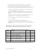
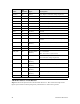
Table 14 lists the pin assignments for the FT 6000 Smart Transceiver. All digital inputs are
low-voltage transistor-transistor logic (LVTTL) compatible, 5 V tolerant, with low leakage.
All digital outputs are slew-rate limited to reduce Electromagnetic Interference (EMI)
concerns.
34 Hardware Resources