
User Manual


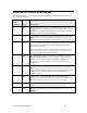


Checklist 5: Device PCB Layout
This checklist applies to all Series 6000 chips, including FT 6000 Smart Transceivers and
Neuron 6000 Processors.
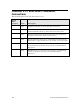
Check
When
Complete Item Description
LO1 Your design incorporates a “star ground” layout design, with the
network connector, coupling circuit, power supply input, and
externally-accessible I/Os all grouped near each other along one
edge (or two adjacent edges) of the PCB.
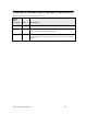
LO2 If your device has a metal enclosure, the enclosure is tied to the
center of the star ground through a low inductance connection
(optionally with a low-inductance DC blocking capacitor in series).
LO3 For 4-layer PCBs, the internal ground plane is used to connect the
center of the star ground out to the ground connections of the
other functional blocks.
For 2-layer PCBs, ground pours on the bottom and top layers are
used to connect the center of the star ground out to the ground
connections of the other functional blocks.
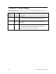
LO5 For FT 6000 Smart Transceiver devices, the EMC keepout area
shown in Figure 30 has no traces or planes in the area shown,
except for the connections from the NETA and NETB traces
through the coupling capacitors and into the communication
transformer.
LO6 There is a low-inductance ground path from the Series 6000 chip
back to the center of the star ground, to ensure that ESD and
surge transients clamped inside the Series 6000 chip have a good
return path back off of the PCB without going through any
sensitive circuitry.
LO7 If the device has a host microprocessor or any other digital
circuitry that could generate RF noise, that circuitry is kept away
from the network cable, power cable, and any I/O cables.
LO8 The leakage capacitance to external metal surfaces from high
frequency circuit traces is controlled with guard traces.
LO9 The FT-X3 Communications Transformer PCB layout matches
Figure 52.
Series 6000 Chip Data Book 125