
User Manual

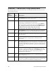

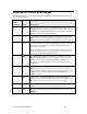


Checklist 1: Series 6000 Chip Connections
This checklist applies to all Series 6000 chips, including FT 6000 Smart Transceivers and
Neuron 6000 Processors.
Check
When
Complete Item Description
CC1 The VDD3V3 pins (8, 18, 29, 30, 41, and 42) are connected to V
DD3
(+3.3 V), as described in Pin Connections.
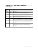
CC2 The VDD1V8 pins (6, 16, and 44) are connected to the VOUT1V8
pin (27) only, as described in Pin Connections.
Do not connect an external 1.8 V source to any of the VDD1V8
pins (6, 16, and 44). Connect these pins to the VOUT1V8 pin (27)
only. Using an external 1.8 V source for the VDD1V8 pins
voids the warranty for the chip, and can cause
unpredictable and possibly irreparable results.
CC3 The AVDD3V3 pin (31) are connected to analog V
DD3
(if separate
from digital V
DD3
) or to +3.3 V, as described in Pin Connections.
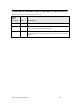
CC4 The chip’s pad (pin 49) is connected to logic ground, as described in
Pin Connections.
CC5 The AGND pin (33) is connected to analog ground (if separate
from logic ground) or to logic ground, as described in Pin
Connections.
CC6 Decoupling capacitors are placed between V
DD3
and ground (0.1 µF
10% 16V X7R) for pins 6, 8, 16, 18, 27, 29, 30, 31, 41, and 44. Each
capacitor is placed directly adjacent to a V
DD3
pin, on the top layer
of the PCB, with a short connection to ground, as described in Pin
Connections.
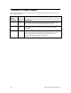
CC7 An additional decoupling capacitor is placed between V
DD3
and
ground (0.1 µF 10% 6.3V X7R) for the VOUT1V8 pin (27). The
capacitor is placed directly adjacent to the VOUT1V8 pin, on the
top layer of the PCB, with a short connection to ground, as
described in Pin Connections.
CC8 Unused I/O pins are pulled up to V
DD3
, or pulled down to ground,
with a 10 kΩ resistor.
CC9 The crystal or oscillator is connected to the XIN and XOUT pins
(23 and 24), is 10 MHz, is 18 pF parallel resonant, and meets the
accuracy requirements described in Clock Requirements.
120 Series 6000 Design Checklists