
Hardware Owner's manual


Table Of Contents
- Welcome
- Audience
- Related Documentation
- FTXL Hardware Overview
- FTXL Developer’s Kit Hardware
- FTXL Transceiver Hardware Interface
- FPGA Design for the FTXL Transceiver
- Working with the Altera Development Environments
- Using the Bring-Up Application to Verify FTXL Hardware Design
- Index
FTXL Hardware Guide 49
• 8 MB CFI flash memory
• 16 MB SDRAM
These numbers correspond to the external memory provided by the DBC2C20
development board. Your FTXL device design can include as much external
memory as required for your device.
Addressing, Size, and IRQ Requirements
For the FTXL Developer’s Kit reference design, the address assignments for the
instruction master and data master components were assigned by allowing the
Altera SOPC Builder tool to allocate and assign the address locations.
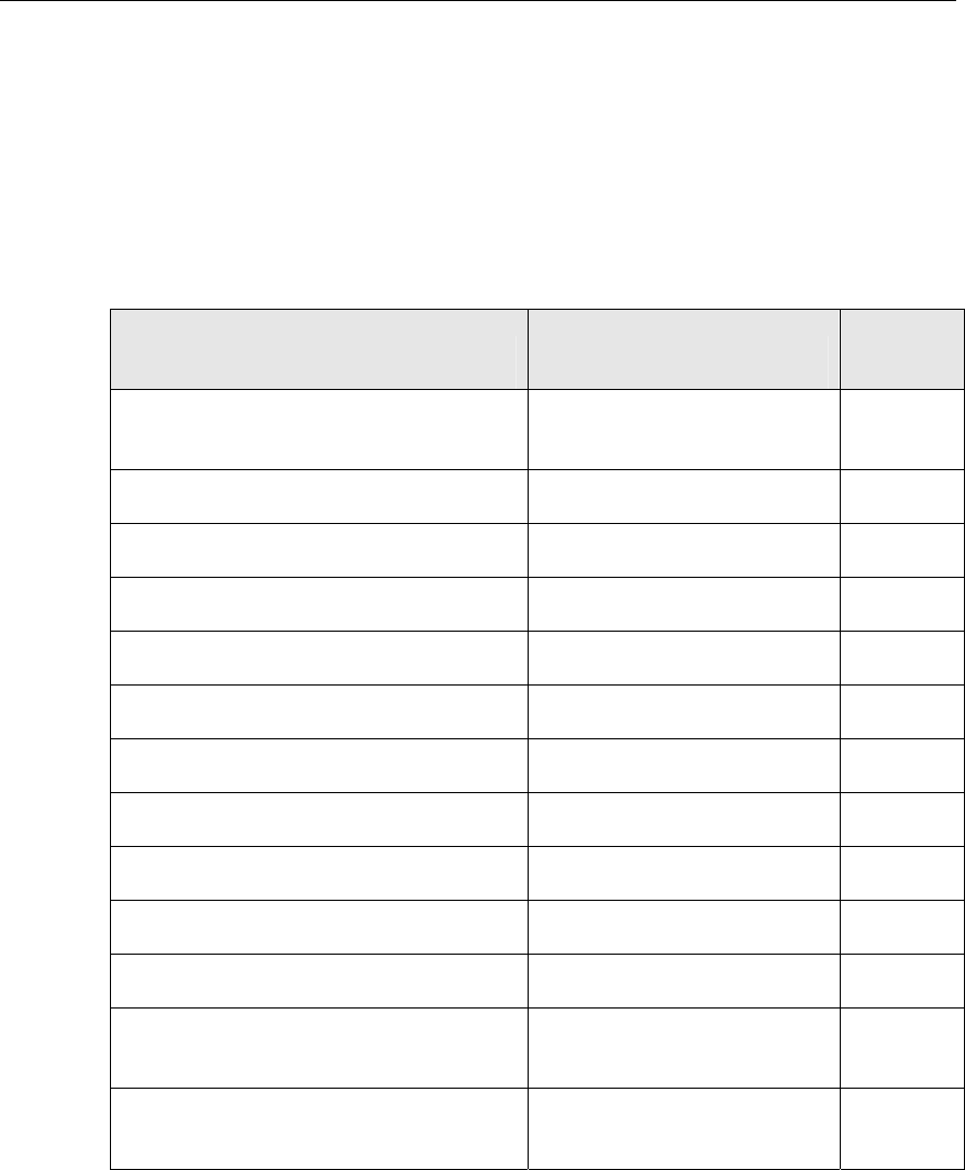
Table 15 lists the size requirements of each of the major components of the FTXL
Developer’s Kit reference design. The size specifications for general components
are the default sizes; the size specifications for the components whose names
begin with FTXL_ define the requirements for the hardware interface.
Table 15. Size Requirements for Components in the FTXL Reference Design
Component Component Name
Size
(Bytes)
FTXL Parallel I/O Transceiver
interface
FTXL_PIO_inst 8
JTAG UART jtag_uart 8
System ID sysid 8
FTXL service LED FTXL_SERVICE_LED_inst 16
FTXL service pin FTXL_SERVICE_PIN_inst 16
FTXL Transceiver interrupt FTXL_IRQ_inst 16
FTXL Transceiver reset FTXL_RESET_inst 16
High-resolution timer high_res_timer 32
System timer sys_timer 32
EPCS serial flash controller port epcs_controller 2 KB
JTAG debug module cpu.jtag_debug_module 2 KB
SRAM interface for the DBC2C20
development board
DBC2C20_sram_interface_0 1 MB
CFI flash interface for the DBC2C20
development board
cfi_flash 8 MB