
Hardware Owner's manual

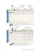
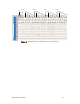


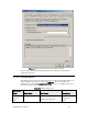
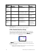
Table Of Contents
- Welcome
- Audience
- Related Documentation
- FTXL Hardware Overview
- FTXL Developer’s Kit Hardware
- FTXL Transceiver Hardware Interface
- FPGA Design for the FTXL Transceiver
- Working with the Altera Development Environments
- Using the Bring-Up Application to Verify FTXL Hardware Design
- Index

42 FPGA Design for the FTXL Transceiver
Component
Name
Class Name File Names Description
FTXL Parallel
I/O
Transceiver
Interface
FTXL_PIO FTXL_PIO_hw.tcl Parallel I/O
interface to the
FTXL Transceiver
FTXL Service
LED
FTXL_SERVICE_LED
FTXL_SERVICE_LED.vhd
FTXL_SERVICE_LED_hw.tcl
Service LED for
the FTXL device
FTXL Service
Pin
FTXL_SERVICE_PIN FTXL_SERVICE_PIN.vhd
FTXL_SERVICE_PIN_hw.tcl
FTXL service pin
input and
interrupt
FTXL
Transceiver
Interrupt
FTXL_IRQ FTXL_IRQ.vhd
FTXL_IRQ_hw.tcl
Interrupt signal
from the FTXL
Transceiver
FTXL
Transceiver
Reset
FTXL_RESET FTXL_RESET.vhd
FTXL_RESET_hw.tcl
Bidirectional reset
signal used to
reset and detect
reset on the FTXL
Transceiver
None of these components has any parameters that you can set within the Altera
SOPC Builder tool.
The following sections describe each of the FTXL components.
FTXL Parallel Interface Delay
Because the Cyclone II FPGA device has low delay times for its signals, the
required timing for the parallel interface control port is achieved by adding a
separate time-delay function to the Quartus II design.
Figure 18 shows the
Quartus II design view of the FTXL parallel interface delay component.
CS_IN
CLK_IN
RESET_IN
A
0_IN
RW_IN
A
0_OUT
CS_OUT
RW_OUT
FTXL_PIO_Delay
inst2
Figure 18. Quartus II Component for the FTXL Parallel Interface Delay
The delay circuit includes six D flip-flops, which provide the required delay for
the three control signals:
• The CS~ signal is delayed by three clock cycles. It is also inverted by a
NAND gate to ensure that it is active low.