
Hardware Owner's manual
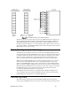
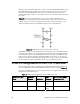

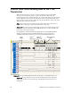
Table Of Contents
- Welcome
- Audience
- Related Documentation
- FTXL Hardware Overview
- FTXL Developer’s Kit Hardware
- FTXL Transceiver Hardware Interface
- FPGA Design for the FTXL Transceiver
- Working with the Altera Development Environments
- Using the Bring-Up Application to Verify FTXL Hardware Design
- Index

30 FTXL Transceiver Hardware Interface
and A0, and waits for the assertion of D0/HS, and then deasserts A0, asserts CS~
and reads D0-D7 to receive the data.
Figure 9 shows an overview example logic analyzer trace
1
of the timing control
flow when the host receives data from the FTXL Transceiver. In this example,
the host receives a query status request.
See Appendix
A,
Using the Bring-Up Application to Verify FTXL Hardware
Design
, on page 63, for more detailed information about verifying the
communications between the host processor and the FTXL Transceiver.
Figure 9. Overview Timing Diagram: Host Receives Data from the FTXL Transceiver
Figure 10 on page 31 shows a more detailed timing diagram for reading the
length byte. The diagram also shows the read handshake.
1
The logic analyzer traces were generated using the TechTools DigiView™ Logic Analyzer.