
Hardware Owner's manual
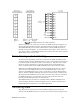
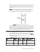
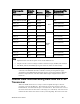
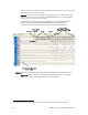

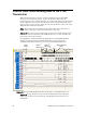
Table Of Contents
- Welcome
- Audience
- Related Documentation
- FTXL Hardware Overview
- FTXL Developer’s Kit Hardware
- FTXL Transceiver Hardware Interface
- FPGA Design for the FTXL Transceiver
- Working with the Altera Development Environments
- Using the Bring-Up Application to Verify FTXL Hardware Design
- Index

FTXL Hardware Guide 29
FPGA Design Pin
Name
FPGA Pin
Number
Direction
Edge
Capture
Corresponding FTXL
Transceiver Pin
FTXL_RESET G16 Bidirectional
Falling
edge
Pin 40 (RESET~)
FTXL_SERVICE_LED U8 Output N/A
FTXL_AO H14 Output Pin 27 (IO10/A0)
FTXL_CS H15 Output Pin 31 (IO8/CS~)
FTXL_RW H16 Output
N/A
Pin 30 (IO9/R/W~)
FTXL_D0 P15 Bidirectional
Pin 4 (IO0/D0/HS)
FTXL_D1 J14 Bidirectional
Pin 3 (IO1/D1)
FTXL_D2 F14 Bidirectional
Pin 2 (IO2/D2)
FTXL_D3 J15 Bidirectional
Pin 43 (IO3/D3)
FTXL_D4 F15 Bidirectional
Pin 42 (IO4/D4)
FTXL_D5 H17 Bidirectional
Pin 36 (IO5/D5)
FTXL_D6 E18 Bidirectional
Pin 35 (IO6/D6)
FTXL_D7 G17 Bidirectional
Either
edge
Pin 32 (IO7/D7)
Notes:
• Signal direction is from the point of view of the FPGA device.
• All pins use the 3.3 V low-voltage transistor-transistor logic (LVTTL) I/O standard.
• The FTXL_AO and the FTXL_D[7..0] pins share an Avalon tri-state bridge.
The FPGA design also defines the pin assignments for the clock signals, SDRAM
controller, and CFI flash interface controller. These pin assignments apply
specifically to the DBC2C20 development board; your design will have different
hardware requirements, and thus define different pin assignments for these
functions.
Control Flow: Host Receiving Data from the FTXL
Transceiver
When the FTXL Transceiver is ready to send an uplink message to the host
program, it asserts the IRQ pin. The host then asserts the A0 pin to read the
handshake bit, and deasserts the pin to read data bit 0. The transceiver receives
the write token after the host writes a message (or a null token). The transceiver
informs the host that it has data to send by asserting IRQ. The host asserts CS~