
Hardware Owner's manual

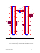

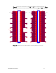
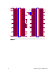


Table Of Contents
- Welcome
- Audience
- Related Documentation
- FTXL Hardware Overview
- FTXL Developer’s Kit Hardware
- FTXL Transceiver Hardware Interface
- FPGA Design for the FTXL Transceiver
- Working with the Altera Development Environments
- Using the Bring-Up Application to Verify FTXL Hardware Design
- Index
14 FTXL Developer’s Kit Hardware
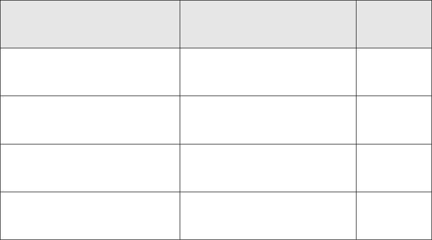
Table 7. FTXL Adapter Board Connectors and Headers
FTXL Developer’s Kit Function FTXL Adapter Board Function
FTXL
Adapter
Board Name
Connects FTXL Adapter Board with
FTXL Transceiver Board for FTXL
Transceiver Chip I/O
Hirose stacking header J1
Connects FTXL Adapter Board with
FTXL Transceiver Board for FTXL
Transceiver Chip I/O
Hirose stacking header J2
Provides access to FTXL Transceiver
Chip I/O
Header and connector for FTXL
Transceiver Chip I/O with
DBC2C20 development board
J5
Provides access to FTXL Transceiver
Chip I/O
Header and connector for FTXL
Transceiver Chip I/O with
DBC2C20 development board
J7
In addition, the FTXL Adapter Board provides an area for prototyping or
measurement through headers J6 and J8, which correspond functionally to
headers J5 and J7. See
Figure 3 on page 12 for the pin assignments of the
DBC2C20 development board headers P22 and P23, which directly connect to the
FTXL Adapter Board headers J5 and J7.
Figure 4 on page 15 shows the connections for the J1 and J2 Hirose stacking
headers. Note that the FTXL Developer’s Kit does not use the connections for
pins 36-44 or pin 81 on the J2 header.