
User guide

Chapter 3 - Input/Output Interfaces
48 FT 3120 / FT 3150 Smart Transceiver Data Book
Notes:
1. Refer to the FT 3120 and FT 3150 Smart Transceiver Datasheet for detailed measurement information.
2. For FT Smart Transceiver-to-FT Smart Transceiver operation, bus contention (t
mrdz
, t
sawdd
) is eliminated by firmware, ensuring that a zero state
is present when the token is passed between the master and slave. See Parallel I/O Interface to the Neuron Chip engineering bulletin for fur-
ther information.
3. HS high is used as a slave busy flag. If HS is held low, the maximum data transfer rate is 24 CLK1s (2.4 µs @ 10MHz) per byte. If HS is not
used for a flag, caution should be taken to ensure the master does not initiate a data transfer before the slave is ready.
4. Parameters were added in order to aid interface design with the FT Smart Transceiver.
6. Master will hold output data valid during a write until the Slave device pulls HS low.
7. CLK1 represents the period of the FT Smart Transceiver input clock (100 ns at 10MHz).
8. In a master read, CS
pulsing low acts like a handshake to flag the slave that data has been latched in.
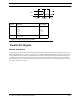
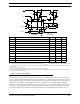
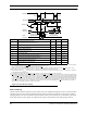
Figure 3.17 Master Mode Timing
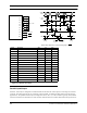
Symbol Description Min Typ Max
t
mrws
R/W setup before falling edge of CS 150 ns 3 CLK1 —
t
mrwh
R/W hold after rising edge of CS 100 ns — —
t
mcspw
CS pulse width 150 ns 2 CLK1 —
t
mhsh
HS hold after falling edge of CS 0 ns — —
t
mhsv
HS checked by firmware after rising edge of CS 150 ns 10 CLK1 —
t
mrdz
Master three-state DATA after rising edge of R/W (Notes 1, 2) — 0 25 ns
t
mrds
Read data setup before falling edge of HS (Note 3) 0 ns — —
t
mhscs
HS low to falling edge of CS (Note 4) 2 CLK1 6 CLK1 —
t
mrdh
Read data hold after falling edge of CS 0 ns — —
t
mwdd
Master drive of DATA after falling edge of R/W (Note 1) 150 ns 2 CLK1 —
t
mhsdv
HS low to data valid (Note 4) — 50 ns —
t
mwds
Write data setup before rising edge of CS 150 ns 2 CLK1 —
t
mwdh
Write data hold after rising edge of CS (Note 6) Note 1 — —
t
mcspw
CS
HS
R/W
DATA OUT
DATA IN
READ CYCLE WRITE CYCLE
t
mhsv
t
mhsh
t
mhsv
t
mrws
t
mrdz
t
mwds
t
mwdh
t
mwdd
t
mrdh
t
mrds
t
mrwh
t
mhscs
t
mhsdv
t
mcspw
t
mhsh
t
mrws