FT 3120® / FT 3150® Smart Transceiver Data Book @ ® 005-0139-01D
Echelon, LON, LONWORKS, Neuron, 3120, 3150, LonTalk, NodeBuilder, LNS, LonMaker, i.LON, and the Echelon logo are trademarks of Echelon Corporation registered in the United States and other countries. Other brand and product names are trademarks or registered trademarks of their respective holders.
Table of Contents Chapter 1 - Introduction ......................................................................................1 Introduction .......................................................................................................2 Audience ...........................................................................................................2 Product Overview .............................................................................................
Table of Contents Direct I/O Objects ..........................................................................................40 Bit Input/Output ........................................................................................40 Byte Input/Output .....................................................................................41 Leveldetect Input ......................................................................................43 Nibble Input/Output ........................................
Chapter 4 - Hardware Design Considerations .................................................91 Introduction .....................................................................................................92 Quick Start for Users Familiar With The FTT-10A Transceiver ...................92 Interface Between Smart Transceivers and the Network ................................93 PC Board Layout Guidelines ..........................................................................95 EMI Design Issues ........
Table of Contents Appendix C - Design and Handling Guidelines .............................................129 Application Considerations ...........................................................................130 Termination of Unused Pins ...................................................................130 Avoidance of Damaging Conditions .......................................................130 Power Supply, Ground, and Noise Considerations .................................
1 Introduction FT 3120 / FT 3150 Smart Transceiver Data Book 1
Chapter 1 - Introduction Introduction This manual provides detailed technical specifications on the electrical interfaces, mechanical interfaces, and operating environment characteristics for the FT 3120® and FT 3150® Smart Transceivers. This manual also provides guidelines for migrating applications to an FT Smart Transceiver-based device using a LonBuilder® or NodeBuilder®development tool.
Product Overview Table 1.1 FT Smart Transceiver Product Offerings Smart Transceiver IC Product Number Model Number FT 3120-E4S40 FT 3120-E4P40 FT 3150-P20 Maximum input clock EEPROM (Kbytes) RAM (Kbytes) ROM (Kbytes) External memory interface 14212R-500 40MHz 4Kbytes 2Kbytes 12Kbytes No 32 SOIC 14222R-800 40MHz 4Kbytes 2Kbytes 12Kbytes No 44 TQFP 14230R-450 20MHz 0.
Chapter 1 - Introduction The FT Smart Transceivers also provide electrical isolation for I/O devices that are grounded, allowing such devices to be used on a link power network segment. In many applications, some I/O devices are grounded, either to meet functional requirements or safety regulations. The FT-X1or FT-X2 transformer electrically isolates the device from the segment, allowing I/O circuitry to be grounded without impairing communications.
Related Documentation Unlike bus wiring designs, the free topology FT Smart Transceivers use a wiring scheme that supports star, loop, and/ or bus wiring (see Figure 1.3). This design has many advantages: 1. The installer is free to select the method of wiring that best suits the installation, reducing the need for advanced planning and allowing last minute changes at the installation site. 2.
Chapter 1 - Introduction LONMARK™ Layers 1-6 Interoperability Guidelines (078-0014-01) LONMARK™ Application Layer Interoperability Guidelines (078-0120-01) FT 3120 and FT 3150 Smart Transceiver Datasheet (003-0337-01) LONWORKS FTT-10A Free Topology Transceiver data sheet (003-0312-01) LONWORKS Custom Node Development engineering bulletin (005-0024-01) LPI-10 Link Power Interface Module User’s Guide (078-0104-01) LPT-10 Link Power Transceiver User's Guide (078-0105-01) Junction Box and Wiring Guidelines for
2 Hardware Resources FT 3120 / FT 3150 Smart Transceiver Data Book 7
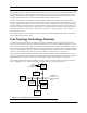
Chapter 2 - Hardware Resources Overview The FT 3150 Smart Transceiver supports external memory for more complex applications, while the FT 3120 Smart Transceiver is a complete system on a chip. The major hardware blocks of both processors are the same, except where noted in the table and figure below. Table 2.
Neuron Processor Architecture Processor 2 is the network processor that implements layers 3 through 6 of the LonTalk protocol stack. It handles network variable processing, addressing, transaction processing, authentication, background diagnostics, software timers, network management, and routing functions. Processor 2 uses network buffers in shared memory to communicate with Processor 1, and application buffers to communicate with Processor 3. These buffers are also located in shared RAM memory.
Chapter 2 - Hardware Resources address, data, and R/W signals are reflected on the corresponding external lines when utilized by any of the internal processors. Each CPU minor cycle consists of three system clock cycles, or phases; each system clock cycle is two input clock cycles. The minor cycles of the three processors are offset from one another by one system clock cycle, so that each processor can access memory and ALUs once during each instruction cycle. Figure 2.
Neuron Processor Architecture addresses for CALL instructions, and may also be used for temporary data storage. This stack architecture leads to very compact code. Tables 2.3, 2.42.4, and 2.5 outline the instruction set. Figure 2.4 shows the layout of a base page, which may be up to 256 bytes long. Each of the three processors uses a different base page, whose address is given by the contents of the BP register of that processor.
Chapter 2 - Hardware Resources Table 2.3 Program Control Instructions Mnemonic Cycles Size (bytes) Description Comments NOP 1 1 No operation SBR 1 1 Short unconditional branch Offset 0 to 15 BR/BRC/ BRNC 2 2 Branch, branch on (not) carry Offset -128 to +127 SBRZ/SBRNZ 3 1 Short branch on TOS (not) zero Offset 0 to 15. Drops TOS BRF 4 3 Unconditional branch far Absolute address BRZ/BRNZ 4 2 Branch on TOS (not) zero Offset -128 to +127.
Memory Allocation POPD [PTR] 6 1 Pop to 16-bit pointer [0 to 3], low byte first PUSH/POP [PTR][TOS] 6 1 EA = (16-bit pointer) + TOS PUSH/POP [PTR][D] 7 2 EA = (16-bit pointer) + displacement [0 to 255] PUSH/POP absolute 7 3 Absolute memory address 7 + 4n 1 Fast I/O instruction, transfer n bytes IN/OUT Table 2.
Chapter 2 - Hardware Resources — Unique 48-bit Neuron ID (written at the factory). — User-written application code and read-mostly data. See Table 2.6 for available EEPROM space. • 2,048 bytes of static RAM that store the following: — Stack segment, application, and system data. — Network and application buffers. • The processor can access 59,392 bytes of the available 65,536 bytes of memory address space via the external memory interface.
Memory Allocation • • Unique 48-bit Neuron ID. Optional user-written application code and data tables. All but 8 bytes of the EEPROM can be written under program control using an on-chip charge pump to generate the required programming voltage. The charge pump operation is transparent to the user. The remaining 8 bytes are written during manufacture, and contain a unique 48-bit identifier for each part called the Neuron ID, plus 16 bits for the device code of the chip manufacturer.
Chapter 2 - Hardware Resources Static RAM Both FT Smart Transceivers contain 2048 bytes of static RAM. The RAM is used to store the following: • • Stack segment, application, and system data Network buffers and application buffers The RAM state is retained as long as power is applied to the device. After reset, releasing the FT Smart Transceiver initialization sequence will clear the RAM (see the section Reset Processes and Timing, later in this chapter).
Input/Output Table 2.7 External Memory Interface Pins Pin Designation Direction Function A0 – A15 Output Address Pins D0 – D7 Input/Output Data Pins E Output Enable Clock R/W Output Read/Write Select Low The preferred method of interfacing the FT Smart Transceiver to another MPU is through the 11 I/O pins using a serial or parallel connection, or through a dual-ported RAM device such as the Cypress CY7C144, CY7C138, or CY7C1342.
Chapter 2 - Hardware Resources System Clock Divide Chain IO6 IO5 IO4 IO3 MUX IO7 System Clock Divide Chain Control Logic Timer/Counter 1 Control Logic Timer/Counter 2 IO2 IO1 IO0 Figure 2.7 Timer/Counter Circuits Clock Input The FT Smart Transceivers operate with an input clock of 5, 10, or 20MHz. The FT 3120 Smart Transceiver also supports 40MHz operation. Developers who are using the LonBuilder 3.0.1 or NodeBuilder 1.
Additional Functions CLK1 CLK 2 Rf R EXTERNAL CRYSTAL C C Figure 2.8 Smart Transceiver Clock Generator Circuit PWHIGH VDD /2 PWLOW VDD /2 VDD /2 Figure 2.9 Test Point Levels for CLK1 Duty Cycle Measurements The FT 3120 Smart Transceiver was designed to run at frequencies up to 40MHz using an external clock oscillator. External oscillators generally take several milliseconds to stabilize after power-up.
Chapter 2 - Hardware Resources • • Software command either the from the application program or from the network. LVI circuit detects a drop in the power supply below a set level. During any of the reset functions, when the RESET pin is in the low state, the FT Smart Transceiver pins go to the states described in the list below. Figure 2.11 also illustrates the condition of the pins during reset and the FT Smart Transceivers initialization sequence after reset is returned high again.
Additional Functions Software Controlled Reset When the CPU watchdog timer expires, or a software command to reset occurs, the RESET pin is pulled low for 256 CLK1 clock cycles. The RESET pin and external capacitor (100 ≤ x ≤ 1000 pF) are allowed to begin charging and provide the required duration of reset. Smart Transceiver 5V VDD To Other Devices IN LVI RESET GND If using flash, an external pulse-stretching LVI must be used (Dallas DS1233-10). Switch RESET CE (100 pF Min 1000 pF Max) Figure 2.
Chapter 2 - Hardware Resources Reset Processes and Timing During the reset period, the I/O pins are in a high-impedance state. The FT 3150 Smart Transceiver address lines A15 – A0 are forced to 0xFFFF, R/W is forced to 0, and E is forced to 1. The data lines are undetermined but driven high or low, so they will not float and draw excess current. The SERVICE pin is high impedance during reset.
Specified by Application Specified by Application Additional Functions Scheduler Init One-Second Timer Init Checksum Init Comm Port Init Stable R/W Reflecting Firmware Execution Random Number Seed Calc Stable Data Reflecting Firmware Execution Stable Address Reflecting Firmware Execution Oscillates at Divide by 2 of CLK1 Oscillates Pull-Ups Enabled System RAM Setup Off-Chip RAM State Init SERVICE Pin Init Stack Init and BIST Oscillator Stabilization* Low R/W Reset WARNING: NOT TO SCALE Outp
Chapter 2 - Hardware Resources • • One-second timer initialization Scheduler initialization During internal oscillator start up (after power up), the FT Smart Transceiver waits for the oscillator signal amplitude to grow before using the oscillator waveform as the system clock. This period depends on the type of oscillator used and its frequency, and begins as soon as power is applied to the oscillator and is independent of the RESET pin.
Additional Functions • • • State wait — wait for the device to leave the applicationless state. • I/O pin initialization step — initialize I/O pins based on application definition. Prior to this point, I/O pins are high impedance. • State wait II — wait for the device to leave the unconfigured or hard-offline state. If waiting was required, a flag is set to indicate that the device should come up offline.
Chapter 2 - Hardware Resources System RAM Setup Communication Port Initialization Checksum Initialization One-Second Timer Initialization Scheduler Initialization Total 2.7 ms 0 ms 10.8 ms 0.61 ms 0.74 ms 53.7 ms Table 2.
Additional Functions SERVICE Pin The SERVICE pin alternates between input and open-drain output at a 76 Hz rate with a 50% duty cycle. When it is an output, it can sink 20 mA for use in driving a LED. When it is used exclusively as an input, it has an optional onchip pull-up to bring the input to an inactive-high state for use when the LED and pull-up resistor are not connected.
Chapter 2 - Hardware Resources Table 2.10 Service LED Behavior During Different States Device State 0xF015 State Code Service LED Applicationless and Unconfigured 3 On Unconfigured (but with an Application) 2 Flashing Configured, Hard Offline 6 Off Configured 4 Off 3150 Defective External Memory — On The SERVICE pin is active low and the service pin message is sent once maximum per SERVICE pin transition.
Integrity Mechanisms The system image checksum covers the system image. It is only available when the system image resides in off-chip memory and its use is optional. A system image checksum error always forces the device to the applicationless state. No checksum is computed if the device is in the applicationless state. The checksums are all verified during reset processing by the network processor and as part of the background diagnostic process.
Chapter 2 - Hardware Resources When an EEPROM recovery occurs due to a checksum failure or other error, the event will be logged in the error table of the FT Smart Transceiver. A test command will show EEPROM recovery occurred as the last error logged. Reset Processing During reset processing, the configuration checksum is checked first.
3 Input/Output Interfaces FT 3120 / FT 3150 Smart Transceiver Data Book 31
Chapter 3 - Input/Output Interfaces Overview The FT 3120 and FT 3150 Smart Transceivers connect to application-specific external hardware via 11 pins, named IO0-IO10. These pins may be configured in numerous ways to provide flexible input and output functions with minimal external circuitry. The programming model (Neuron C language) allows the programmer to declare one or more pins as I/O objects.
Hardware Considerations Hardware Considerations Tables 3.1 through 3.5 list the 34 different I/O objects available. Various I/O objects of different types may be used simultaneously. Figure 3.3 summarizes the pin configuration for each of the I/O objects. For the electrical characteristics of these pins, refer to the FT 3120 and FT 3150 Smart Transceiver Datasheet. The following sections contain detailed descriptions of all the I/O objects.
Chapter 3 - Input/Output Interfaces Table 3.1 Summary of Direct I/O Objects I/O Object Applicable I/O Pins Input/Output Value Page No.
Hardware Considerations Table 3.4 Summary of Timer/Counter Input Objects Page No. I/O Object Applicable I/O Pins Input Signal Dualslope Input IO0, IO1 + (one of IO4 – IO7) Comparator output of the dualslope converter logic 71 Edgelog Input IO4 A stream of input transitions 72 Infrared Input IO4 – IO7 Encoded data stream from an infrared demodulator 73 Ontime Input IO4 – IO7 Pulse width of 0.2 µs – 1.678 s 74 Period Input IO4 – IO7 Signal period of 0.2 µs – 1.
Chapter 3 - Input/Output Interfaces tsetup 20 ns thold 0 ns Input IO_0 – IO_10 Internal System Clock (200 ns pulse with 10MHz Input Clock) Figure 3.
I/O Timing Issues 0 I/O Pin DIRECT I/O OBJECTS 1 2 3 4 5 6 7 8 9 10 Bit Input, Bit Output All Pins 0 – 7 Byte Input, Byte Output Leveldetect Input Any Four Adjacent Pins Nibble Input, Nibble Output PARALLEL I/O OBJECTS Parallel I/O Muxbus I/O Data Pins 0 – 7 Master/Slave A Data Pins 0 – 7 CS R/W HS Slave B Data Pins 0 – 7 CS R/W A0 Bitshift Input, Bitshift Output C D I2C I/O Magcard Input SERIAL I/O OBJECTS Magtrack1 Input Neurowire I/O Master Slave C D C D ALS WS RS C
Chapter 3 - Input/Output Interfaces • The FT Smart Transceiver hardware The contribution of the scheduler to the overall timing characteristic is approximately uniform across all 34 I/O function blocks since its contribution to the overall I/O timing is at a relatively high functional level. The contribution of firmware and hardware varies from one I/O object to another (e.g., Bit I/O versus Neurowire I/O), with one area generally being the dominant factor.
I/O Timing Issues IO_out call IO_out call tww IO_out call tww tsol IO_0 TIME 1st when clause end-of-loop processing begins 2nd when clause 1st when clause (Not to scale) Symbol Description Typ @ 10MHz tww when-clause to when-clause latency 940 µs tsol Scheduler overhead latency (see text) 54 µs Figure 3.
Chapter 3 - Input/Output Interfaces Direct I/O Objects The timing numbers shown in this section are valid for both an explicit I/O call or an implicit I/O call through a when clause, and are assumed to be for a FT Smart Transceiver running at 10MHz. Bit Input/Output Pins IO0 – IO10 may be individually configured as single-bit input or output ports. Inputs may be used to sense TTLlevel compatible logic signals from external logic, contact closures, and the like.
Direct I/O Objects tfin tret INPUT TIME START OF io_in() INPUT PIN SAMPLED END OF io_in() Symbol Description Typ @ 10MHz tfin Function call to sample IO0 – IO10 41 µs tret Return from function IO0 IO1 IO2 IO3 IO4 IO5 IO6 IO7 IO8 IO9 IO10 19 µs 23.4 µs 27.9 µs 32.3 µs 36.7 µs 41.2 µs 45.6 µs 50 µs 19 µs 23.4 µs 27.9 µs Figure 3.
Chapter 3 - Input/Output Interfaces control and addressing. See Figures 3.8, 3.9, and 3.10. The IO0 represents the LSB of data. The direction of a byte port may be changed between input and output dynamically under application control. IO0 IO1 IO2 IO3 IO4 IO5 IO6 IO7 IO8 IO9 IO10 IO0 IO1 IO2 IO3 IO4 IO5 IO6 IO7 IO8 IO9 IO10 High Current Sink Drivers Optional Pull-Up Resis- Figure 3.
Direct I/O Objects Leveldetect Input Pins IO0 – IO7 may be individually configured as leveldetect input pins, which latch a negative-going transition of the input level with a minimal low pulse width of 200ns, with a FT Smart Transceiver clocked at 10MHz. The application can therefore detect short pulses on the input which might be missed by software polling. This is useful for reading devices, such as proximity sensors. This is the only direct I/O object which is latched before it is sampled.
Chapter 3 - Input/Output Interfaces Nibble Input/Output Groups of four consecutive pins between IO0 – IO7 may be configured as nibble-wide input or output ports, which may be read or written to using integers in the range 0 to 15. This is useful for driving devices that require BCD data, or other data four bits at a time.
Parallel I/O Objects tfout tret OUTPUT TIME START OF io_out() OUTPUT PIN UPDATED Symbol Description Typ @ 10MHz tfout Function to update IO0 IO1 IO2 IO3 IO4 78 µs 89.8 µs 101.5 µs 113.3 µs 125 µs tret Return from function IO0 – IO4 5 µs END OF io_out() Figure 3.
Chapter 3 - Input/Output Interfaces ADDR/ DATA DATA ADDR tas IO0 DATA ADDR trset tas C_ALS (IO8) IO1 IO2 IO3 twas AD0 – AD7 IO4 tahw tahr tadrs C_RS (IO10) IO5 tdws IO6 IO7 IO8 C_ALS IO9 C_WS IO10 C_RS twrs twhold trhold C_WS (IO9) twws tfout TIME twret START OF io_out() END OF io_out() trret tfin START OF io_in() END OF io_in() NOTE: Data is latched 4.8 µs after the falling edge of C_RS. Symbol Description Min Typ Max tfout io_out() to valid address — 26.
Parallel I/O Objects the slave B configuration, with the other microprocessor as the master. Handshaking is used in both modes to control the instruction execution, and application processing is suspended for the duration of the transfer (up to 255 bytes/ transfer). Consult the Neuron C Reference Guide for detailed programming instructions.
Chapter 3 - Input/Output Interfaces CS tmhscs tmcspw tmcspw tmhsv tmhsh tmhsv tmhsh HS tmrws tmrwh tmrws tmhsdv R/W tmrdz tmwdd tmwdh tmwds DATA OUT tmrds tmrdh DATA IN READ CYCLE Symbol Description WRITE CYCLE Min Typ Max tmrws R/W setup before falling edge of CS 150 ns 3 CLK1 — tmrwh R/W hold after rising edge of CS 100 ns — — tmcspw CS pulse width 150 ns 2 CLK1 — tmhsh HS hold after falling edge of CS 0 ns — — tmhsv HS checked by firmware after rising edge of C
Parallel I/O Objects CS tsahsv tsahsv tsacspw tsacspw tsahsh tsahsh HS tsarws tsarwh tsarws R/W tsawd tsards tsardh DATA IN tsawds tsawdh tsardz DATA OUT WRITE CYCLE (MASTER READ) Symbol Description READ CYCLE (MASTER WRITE) Min Typ Max tsarws R/W setup before falling edge of CS 25 ns — — tsarwh R/W hold after rising edge of CS 0 ns — — tsacspw CS pulse width 45 ns — — tsahsh HS hold after rising edge of CS 0 ns — — tsahsv HS valid after rising edge of CS tsawdd
Chapter 3 - Input/Output Interfaces filled with 0s. The master program writes once to the slave and reads once from the slave. To implement continuous writes and reads, add an io_out_request() function call after the io_in() function call in the master program. /* This is the master program. After reset, the buffer is filled with 1s and then the buffer is written to the slave. The master then reads the slave’s buffer.
Parallel I/O Objects /* This is the slave program. After reset, the output buffer is filled with data and then the slave reads from the master. The slave then writes to the master. The slave’s input buffer should contain [5,1,1,1,1,1]; the output buffer should contain [7,1,2,3,4,5,6,7,0,0,0,0,0,0].
Chapter 3 - Input/Output Interfaces The FT Smart Transceiver may appear as two registers in the address space of the master; one of the registers being the read/write data register, and the other being the read-only status register. Therefore, reads by the master to an odd address access the status register for handshaking acknowledgments and all other reads or writes access the data register for I/O transfers. The LSB of the control register, which is read through pin IO0, is the HS bit.
Parallel I/O Objects Handshaking Handshaking allows the master to monitor the slave between every byte transfer, ensuring that both processors are ready for the byte to be transferred. If the master owns the token, the master waits for the HS from the slave before writing data to the bus. If the slave owns the token, the master monitors the low transition of the HS before reading the bus. In master or slave A mode, the FT Smart Transceiver HS line is pin IO10.
Chapter 3 - Input/Output Interfaces MASTER CS tsbcspw tsbcspw tsbah MASTER A0 tsbas tsbrwh tsbrws MASTER R/W tsbrdh tsbrws LATCH MASTER DATA OUT SLAVE DATA OUT Symbol tsbrds tsbwdz tsbwdv WRITE CYCLE (MASTER READ) Description tsbwdh READ CYCLE (MASTER WRITE) Min Typ Max tsbrws R/W setup before falling edge of CS FT 3120 and FT 3150 Smart Transceivers 0 ns — — tsbrwh R/W hold after rising edge of CS 0 ns — — tsbcspw CS pulse width Note 1 — — tsbas A0 setup to falling edge
Parallel I/O Objects FT SMART TRANSCEIVERS MASTER HAS TOKEN MASTER WRITE DATA PASS TOKEN CMP_ RESYNC WRITE DATA PASS TOKEN CMP_ACK RESYNC SLAVE HAS TOKEN SLAVE Figure 3.21 Handshake Protocol Sequence Between the Master and the Slave Once in possession of the write token, the device (FT Smart Transceiver or a host processor) can transfer up to 255 bytes of data. The stream of data bytes is preceded by the command and length bytes.
Chapter 3 - Input/Output Interfaces Read (length) Write (data_0) . . . Write (data_n) // master begins data transfer to slave Read (data_0) . . . // last byte of data to be transferred Read (data_n) Write EOM // end of data transfer (EOM=0x00) Process EOM// exchange token (Owns Token) Slave writes buffer to master: Enter RD/_WR=1. MASTER SLAVE (Owns Token) Write XFER Read XFER Write (length) Read (length) Write (data_0) Read (data_0) . . . . . .
Serial I/O Objects Serial I/O Objects The timing numbers shown in this section are valid for both an explicit I/O call or an implicit I/O call through a when clause, and are assumed to be for a FT Smart Transceiver running at 10MHz. Bitshift Input/Output Pairs of adjacent pins may be configured as serial input or output lines. The first pin of the pair can be IO0-IO6, IO8, or IO9, and is used for the clock (driven by the FT Smart Transceiver).
Chapter 3 - Input/Output Interfaces INPUT SAMPLED thold tfin taet ttae OUTPUT CLOCK tret DATA IN START OF io_in() END OF io_in() Active clock edge assumed to be positive in the above diagram Symbol Description Typ @ 10MHz tfin Function call to first edge 156.6 µs tret Return from function 5.4 µs thold Active clock edge to sampling of input data 15 kbps bit rate 10 kbps bit rate 1 kbps bit rate 9 µs 40.8 µs 938.
Serial I/O Objects tsetup taet tfin ttae OUTPUT CLOCK tret DATA OUT START OF io_in() END OF io_in() Active clock edge assumed to be positive in the above diagram Symbol Description Typ @ 10MHz tfin Function call to first data out stable 16-bit shift count 1-bit shift count 185.3 µs 337.6 µs tret Return from function 10.8 µs tsetup Data out stable to active clock edge 15 kbps bit rate 10 kbps bit rate 1 kbps bit rate 10.8 µs 10.8 µs 10.
Chapter 3 - Input/Output Interfaces IO0 IO1 IO2 IO3 IO4 IO5 IO6 IO7 IO8 IO9 IO10 SDA Clock Serial Data SDA tdch tstart tcld tchcl SCL tstop tcla SCL tchd tclch tdcl tf TIME TIME INPUT DATA SAMPLED tret START OF io_in() OR io_out() BIT TRANSFER TIMING END OF io_in() OR io_out() START AND STOP TIMING Parameter Description Min Typ Max tf I/O call to start condition io_in() io_out() — — 54.6 µs 43.4 µs — — tstart End of start condition io_in() io_out() 5.4 µs 5.
Serial I/O Objects LSB first. In addition, any one of the pins IO0 – IO7 may be used as a timeout pin to prevent lockup in case of abnormal abort of the input bit stream during the input process. Up to 40 characters may be read at one time. Both the parity and the Longitudinal Redundancy Check (LRC) are checked by the FT Smart Transceiver.
Chapter 3 - Input/Output Interfaces Magtrack1 Input This input object type is used to read synchronous serial data from an ISO3554 magnetic stripe card reader. The data input is on pin IO9, and the clock, or data strobe, is presented as input on pin IO8. The data on pin IO9 is clocked in just following the falling edge of the clock signal on IO7, with the LSB first.
Serial I/O Objects Data are recognized in the IATA format as a series of 6-bit characters plus an even parity bit per character. The process begins when the start sentinel (hex 05) is recognized, and continues until the end sentinel (0x0F) is recognized. No more than 79 characters, including the 2 sentinels and the LRC character, will be read.
Chapter 3 - Input/Output Interfaces thold tsetup thigh tlow CLOCK DATA OUT DATA IN INPUT SAMPLED tfin tcs_clock tclock_cs CLOCK tret SELECT START OF io_in() OR io_out() END OF io_in() OR io_out() Parameter Description Typ tfin Function call to CS active 69.9 µs tret Return from function 7.2 µs thold Active clock edge to sampling of input data 20 kbps bit rate 10 kbps bit rate 1 kbps bit rate 11.4 µs 53.4 µs 960.
Serial I/O Objects the active edge of the clock to negative. One of the IO0 – IO7 pins may be designated as a timeout pin. A logic 1 level on the timeout pin causes the Neurowire slave I/O operation to be terminated before the specified number of bits has been transferred. This prevents the FT Smart Transceiver watchdog timer from resetting the chip in the event that fewer than the requested number of bits are transferred by the external clock. See Figure 3.30.
Chapter 3 - Input/Output Interfaces The chip select logic for the Neurowire slave can be handled by the user through a separate bit input object, along with an appropriate handshaking algorithm implemented by the user application program. In order to prevent unnecessary timeouts, the setup and hold times of the chip select line, relative to the start and end of the external clock, must be satisfied.
Serial I/O Objects The duration of this function call is a function of the number of data bits transferred and the transmission bit rate. tfin (max) refers to the maximum amount of time this function will wait for a start bit to appear at the input. After this time, the function will return a 0 as data. tfin (min) is the time to the first sampling of the input pin. As an example, the timeout period at 2400 bits/second is (20 x 10 x 1/2400) + tfin (min).
Chapter 3 - Input/Output Interfaces IO0 IO1 IO2 IO3 IO4 IO5 IO6 IO7 IO8 IO9 IO10 LINE TYPE LEGEND FT Smart Transceiver TOUCH MEMORY PULL-UP RESISTOR WRITE 1 tf tlow DATA LINE High Current Sink Drivers twrd RESET AND PRESENCE WRITE 0 trsto tpd trstl tpdl twh tibd DATA LINE trdi trret READ DATA LINE DATA LINE tret TIME TIME START OF touch_reset() INPUT SAMPLED END OF touch_reset() START OF io_in() OR io_out() INPUT SAMPLED END OF io_in() OR io_out() Symbol Description Min Typ M
Serial I/O Objects The Touch I/O object can run at FT Smart Transceiver clock rates of 5MHz and 10MHz only. This is because the Touch I/O object is designed to meet the Touch Memory timing specification at those FT Smart Transceiver clock speeds only. The Touch I/O object is not supported at clock rates faster than 10MHz or slower than 5MHz.
Chapter 3 - Input/Output Interfaces IO0 IO1 IO2 IO3 IO4 IO5 IO6 IO7 IO8 IO9 IO10 Optional Pull-Up Resistors tdw DATA A tibd DATA B tfin ttow TIMEOUT ttret tret TIME START OF io_in() END OF io_in() Symbol Description Min Typ Max tfin Function call to start of second data edge — 75.6 µs — tdw Input data width (at 10MHz) 200 ns 100 µs 880 ms tibd Inter-bit delay 150 µs — 900 µs ttow Timeout pulse width — 39 µs — ttret Timeout to function return — 18.
Timer/Counter Input Objects Input timer/counter objects have the advantage (over non-timer/counter objects) in that input events will be captured even if the application processor is occupied doing something else when the event occurs. A true when statement condition for an event being measured by a timer/counter is the completion of the measurement and a value being returned to an event register.
Chapter 3 - Input/Output Interfaces The resolution and range of the timer/counter period options is shown by Table 3.6 in section , Notes, at the end of this chapter.
Timer/Counter Input Objects The resolution and range of the timer/counter period options are shown in Table 3.6 in section , Notes. This object is useful for analyzing an arbitrarily-spaced stream of input edges (or pulses), such as the output of a UPC bar-code reader or infrared receiver.
Chapter 3 - Input/Output Interfaces The infrared input object, based on the input data stream, generates a buffer containing the values of the bits received. The resolution and range of the timer/counter period options is shown in Table 3.6 in section , Notes, at the end of this chapter. This function can be used with an off-the-shelf IR demodulator such as an NEC µPD1913 or Sharp GP1U50X to quickly develop an infrared interface to the FT Smart Transceiver.
Timer/Counter Input Objects IO0 IO1 Event Register IO2 IO3 Timer/Counter 2 IO4 IO5 mux Timer/Counter 1 IO6 IO7 IO8 IO9 IO10 Event Register System Clock Divide Chain Optional Pull-Up Resistors Reference Figure 3.35 Symbol Description Typ @ 10MHz tfin Function call to input sample 86 µs tret Return from function 52/22 µs* *If the measurement is new, tret = 52 µs. If a new time is not being returned, tret = 22 µs. Figure 3.39 Ontime Latency Values This is a level-sensitive function.
Chapter 3 - Input/Output Interfaces IO0 IO1 Event Register IO2 IO3 Timer/Counter 2 IO4 IO5 mux Timer/Counter 1 IO6 IO7 IO8 Event Register IO9 System Clock Divide Chain IO10 Optional Pull-Up Resistors INPUT TIME START TIMER STOP TIMER COUNTER tfin START OF io_in() tret READ TIMER/COUNTER FLAG AND EVENT REGISTER CLEAR FLAG END OF io_in() Reference Figure 3.
Timer/Counter Input Objects Pulsecount Input A timer/counter may be configured to count the number of input edges (up to 65,535) in a fixed time (0.8388608 second) at all allowed input clock rates. Edges may be defined as rising or falling. This object is useful for average frequency measurements, or tachometer applications. See Figure 3.41.
Chapter 3 - Input/Output Interfaces Quadrature Input A timer/counter may be configured to count transitions of a binary Gray code input on two adjacent input pins. The Gray code is generated by devices such as shaft encoders and optical position sensors which generate the bit pattern (00,01,11,10,00, …) for one direction of motion and the bit pattern (00,10,11,01,00, …) for the opposite direction.
Timer/Counter Input Objects A call to this function returns the current value of the quadrature count since the last read operation. The counter is then reset and ready for the next series of input transitions. The count returned is a 16-bit signed binary number, capped at ±16K. The number shown in the diagram above is the minimum time allowed between consecutive transitions at either input of the quadrature function block.
Chapter 3 - Input/Output Interfaces A call to this function returns the current value of the totalcount value corresponding to the total number of active clock edges since the last call. The counter is then reset, and ready for the next series of input transitions. The actual active edge of the input depends on whether or not the invert option was used in the declaration of the function block. The default is the negative edge.
Timer/Counter Output Objects IO0 Timer/Counter 1 IO1 IO2 Timer/Counter 2 Output IO3 IO4 mux IO5 IO6 Sync Input IO7 IO8 IO9 IO10 High Current Sink Drivers Optional Pull-Up Resistors tsod OUTPUT SYNC INPUT tfout TIME START OF io_out() twin tfod tret INTERNAL COUNT BEGINS END OF io_out() START OF io_out() OUTPUT INACTIVE Symbol Description Min Typ Max tfout Function call to start of timer — 96 µs — tfod Function to output disable — 82.
Chapter 3 - Input/Output Interfaces to drive an audio transducer, or to drive a frequency to voltage converter to generate an analog output. See Figure 3.45. IO0 Timer/Counter 1 IO1 IO2 IO3 IO4 Timer/Counter 2 IO5 IO6 IO7 IO8 System Clock Divide Chain IO9 IO10 High Current Sink Drivers Frequency Resolution and Maximum Range at 10MHz ONE CYCLE tfout CLK Resolution Range Unit 0 0.4 26.21 µs 1 0.8 52.42 µs 2 1.6 104.86 µs 3 3.2 209.71 µs 4 6.4 419.42 µs 5 12.8 838.
Timer/Counter Output Objects Oneshot Output A timer/counter may be configured to generate a single pulse of programmable duration. The asserted state may be either logic high or logic low. Retriggering the oneshot before the end of the pulse causes it to continue for the new duration. Table 3.6 in section , Notes, gives the resolution and maximum time of the pulse for various clock selections. This object is useful for generating a time delay without intervention of the application processor. See Figure 3.
Chapter 3 - Input/Output Interfaces Pulsecount Output A timer/counter may be configured to generate a series of pulses. The number of pulses output is in the range 0 to 65,535, and the output waveform is a square wave of 50% duty cycle. This function suspends application processing until the pulse train is complete. The frequency of the waveform may be one of eight values given by Table 3.7 in section , Notes with clock select values of 0 through 7.
Timer/Counter Output Objects Pulsewidth Output A timer/counter may be configured to generate a pulsewidth modulated repeating waveform. In pulsewidth short function, the duty cycle ranges from 0% to 100% (0/256 to 255/256) of a cycle in steps of about 0.4% (1/256). The frequency of the waveform may be one of eight values given by Table 3.7. In pulsewidth long function, the duty cycle ranges from 0% to almost 100% (0/65,536 to 65,535/65,536) of a cycle in steps of 15.25 ppm (1/65,536).
Chapter 3 - Input/Output Interfaces Triac Output On the FT Smart Transceiver, a timer/counter may be configured to control the delay of an output signal with respect to a synchronization input. This synchronization can occur on the rising edge, the falling edge, or both the rising and falling edges of the input signal. For control of AC circuits using a triac device, the sync input is typically a zerocrossing signal, and the pulse output is the triac trigger signal. Table 3.
Timer/Counter Output Objects The hardware update does not happen until the occurrence of an external active sync clock edge. The internal timer is then enabled and a triac gate pulse is generated after the user-defined period has elapsed. This sequence is repeated indefinitely until another update is made to the triac gate pulse delay value. tfout (min) refers to the delay from the initiation of the function call to the first sampling of the sync input.
Chapter 3 - Input/Output Interfaces IO0 IO1 IO2 IO3 IO4 IO5 IO6 IO7 IO8 IO9 IO10 Timer/Counter 1 Timer/Counter 2 mux High Current Sink Drivers Control Output Count Input Optional Pull-Up Resistors tfout tcod OUTPUT SYNC INPUT tret TIME START OF io_out() OUTPUT ACTIVE LAST ACTIVE SYNC CLOCK EDGE END OF io_out() OUTPUT INACTIVE Symbol Description Typ @ 10MHz tfout Function call to output pulse 109 µs tcod Last negative sync Clock edge to output inactive min 550 ns max 750 ns tret Ret
Notes The gradient behavior of the timing numbers for different FT Smart Transceiver pins for some of the I/O objects is due to the shift-and-mask operation performed by the Neuron firmware. For dualslope input, edgelog input, ontime input, and period input, the timer/counter returns a value (or a table of values, in the case of edgelog input) in the range 0 to 65,535, representing elapsed times from 0 up to the maximum range given in Table 3.6.
Chapter 3 - Input/Output Interfaces Table 3.7 Timer/Counter Square Wave Output Clock Select (System Clock ÷) Repetition Rate (Hz) Repetition Period (µs) Resolution of Pulse (µs) 0 (÷1) (5MHz) 19,531 51.2 0.2 1 (÷ 2) (2.5MHz) 9,766 102.4 0.4 2 (÷ 4) (1.25MHz) 4,883 204.8 0.8 3 (÷ 8) (625 kHz) 2,441 409.6 1.6 4 (÷ 16) (312.5 kHz) 1,221 819.2 3.2 5 (÷ 32) (156.25 kHz) 610 1,638.4 6.4 6 (÷ 64) (78.125 kHz) 305 3,276.8 12.8 7 (÷ 128) (39.06 kHz) 153 6,553.6 25.
4 Hardware Design Considerations FT 3120 / FT 3150 Smart Transceiver Data Book 91
Chapter 4 - Hardware Design Considerations Introduction This chapter covers the hardware design considerations for the use of the FT 3120 and FT 3150 Smart Transceivers. These design considerations include the interconnections to the FT Smart Transceiver and the FT-X1or FT-X2 communication transformer, PCB Layout guidelines, and EN 61000-4 EMC immunity testing.
Interface between Smart Transceivers and the Network The T1 and T2 signals are each brought out of the FT-X1 transformer at two different sets of pins. The T1 and T2 connections between the FT-X1 transformer and the FT Smart Transceivers can be made via either set of pins on the FT-X1 transformer, but the connections shown in the PCB layout figures later in this chapter generally give the best ESD transient immunity.
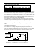
Chapter 4 - Hardware Design Considerations Table 4.1 FT Smart Transceiver External Components Name Value Comments C1 0.1µF for +5VDC decoupling VCC decoupling capacitor for ESD protection diodes D1-D2 VR1 470V MOV, 5mm, 40pF (typ.) Panasonic ERZV05D471, Digi-Key P7186ND or equivalent.
VDD5 VDD5 1 1 PC Board Layout Guidelines FT-3120_CORE FT_CA 1 2 FT_CAR 1 D216A 3 1 1.00K 1% 0603 1 VDD5 P2V5 2 FT_RXS 3 - V+ U204A TLC372 1 + V- TSSOP-8 BAV99 SOT-23 RX- R217 24.9K 1% 0603 1 P2V5 5 FT_TXS 6 + - U205B TLC372 7 TX- TSSOP-8 R219 100K 1% 0603 2 1 C210 0.1uF 16V 10% X7R 0603 2 2 1 D217B 3 2 BAV99 SOT-23 RX- TX- R218 100K 1% 0603 8 R216 24.9K 1% 0603 LED202 LED GREEN 4 COMM_ACTIVE R215 C209 0.
Chapter 4 - Hardware Design Considerations are possible as long as the general principles discussed later in this chapter are followed. Through-hole capacitors and diodes can be used, but SMT components will generally be superior because of their lower series inductance. Electrostatic discharge (ESD) and electromagnetic interference (EMI) are two of the most important design considerations when laying out the PCB for a device. These topics are discussed in general terms at the end of this chapter.
PC Board Layout Guidelines C o m p o n e n t S id e D2 D1 C6 VCC N et C 1 S o ld e r S id e (X -ra y v ie w ) C5 T2 T1 T2 GND T1 GND T2 T2 T1 T1 K e e p -o u t a re a N ET_B S ta r G ro u n d C e n te r N ET_A VR1 C 3 N E T_B N E T_A D 3 D 4 C 4 Figure 4.
Chapter 4 - Hardware Design Considerations S m a rt T r a n s c e iv e r A p p lic a tio n I/ O B lo c k D 1 C 6 D 2 C 5 Pow er S u p p ly B lo c k S ta r G ro u n d C e n te r Figure 4.4 Star Ground Design EMI Design Issues The high-speed digital signals associated with microcontroller designs can generate unintentional electromagnetic interference (EMI).
EMI Design Issues Careful PCB layout is important to ensure that a FT Smart Transceiver based-device will achieve the desired level of EMC. A typical FT Smart Transceiver based-device will have several digital signals switching in the 1-40MHz range. These signals will generate voltage noise near the signal traces, and will also generate current noise in the signal traces and power supply traces.
Chapter 4 - Hardware Design Considerations current flows during Vgate transitions, and more common-mode RF current couples into the network twisted pair. This common-mode RF current can generate EMI in the 30-500MHz frequency range in excess of FCC/CISPR “B” levels, even when Cleak,SIGNAL from a clock line to earth ground is less than 1pF. Guarding of clock lines is essential for meeting Level “B” limits. From this discussion, it should be apparent that minimizing Cleak,SIGNAL is very important.
ESD Design Issues In summary, the following general rules and guidelines apply: • • The faster the FT Smart Transceiver clock speed, the higher the level of EMI. • The FT 3120 Smart Transceiver will generate less EMI than the FT 3150 Smart Transceiver because the FT 3120 Smart Transceiver has no external memory interface lines. • A four-layer PCB will generate less EMI than a two-layer PCB since the extra layers facilitate better VCC decoupling and more effective logic ground guarding.
Chapter 4 - Hardware Design Considerations into the ground plane. If a positive ESD hit discharges into the keypad, then the VCC diodes shunt the current to the ground plane via a 0.1µF decoupling capacitor that is placed directly adjacent to the clamp diodes. The keypad connector, diodes and decoupling capacitor should all be located close to the center of the star ground so that the ESD current does not pass through sensitive circuitry on its way out of the PCB.
Lightning Protection Shield Protection Gas Discharge, MOV, or TVS devices may be used for the shield-to-ground protection. MOV and TVS devices may not be used to protect the network data lines. Suggested Gas Discharge Arresters Three-electrode device configurations are suggested for the data network lines, as this will require the use of only one physical device to protect both lines.
Chapter 4 - Hardware Design Considerations When the network data line extends outside of a building or grounded structure, every FTT-10A and FT 3120 / 3150 Free Topology FT Smart Transceiver-based device on the network segment, whether located indoors or outdoors, must be equipped with surge protection circuitry. Additionally, protection devices must be added to the network at every point where the network cable exits the building or structure.
EN 61000-4 Electromagnetic Compatibility (EMC) Testing For more information on levels and installation classes, see EN 61000-4-5. The applicable surge test levels and coupling mode specified by EN 61000-4-5 can be found in Table A.1 of that document as follows: • • • Balanced circuits/lines; Coupling mode is line-to-ground, either polarity; Surge waveform is 1.2/50µs (8/20µs) combination wave for classes 1-4.
Chapter 4 - Hardware Design Considerations Dressler Alpha 250 / 75W HP8656B SIGNAL GENERATOR EMCO ATT 6 / 75 75W POWER AMP -6dB 75W PAD FCC BCI Termination 50Ω AE POWER FCC CDN - M3 AUXILIARY EQUIPMENT (AE) UTP EQUIPMENT UNDER TEST (EUT) EUT POWER 50Ω FCC CDN - M3 GROUND PLANE GPIB TEST CONTROL COMPUTER FCC BCI - Fischer Custom Communications Bulk Current Injection Probe P/N F-120-9A FCC CDN M3 - Fischer Custom Communications Coupling De-Coupling Network P/N FCC-801-M3-16A Figure 4.
EN 61000-4 Electromagnetic Compatibility (EMC) Testing Dressler Alpha 250 / 75W HP8656B SIGNAL GENERATOR EMCO ATT 6 / 75 75W POWER AMP -6dB 75W PAD FCC BCI Termination 50Ω AE POWER FCC CDN - M3 AUXILIARY EQUIPMENT (AE) STP EQUIPMENT UNDER TEST (EUT) EUT POWER 50Ω FCC CDN - M3 GROUND PLANE GPIB TEST CONTROL COMPUTER FCC BCI - Fischer Custom Communications Bulk Current Injection Probe P/N F-120-9A FCC CDN M3 - Fischer Custom Communications Coupling De-Coupling Network P/N FCC-801-M3-16A Fi
Chapter 4 - Hardware Design Considerations 16.00 80.00 75.00 14.00 70.00 65.00 Amplitude [Vrms] 10.00 60.00 55.00 50.00 45.00 8.00 40.00 FTT-10A Transceiver 6.00 35.00 Amplitude [Vpp] FT 31x0 Smart Transceiver with C5 = C6 = 56pF caps 12.00 30.00 25.00 4.00 20.00 15.00 2.00 10.00 5.00 0.00 0 1 10 0.00 100 Frequency [MHz] Figure 4.
5 Network Cabling and Connections FT 3120 / FT 3150 Smart Transceiver Data Book 109
Chapter 5 - Network Cabling and Connections Network Connection The network connection (NET1 and NET2) is polarity insensitive. Therefore, either of the two twisted pair wires can be connected to either of these network connections. Network Topology Overview The TP/FT-10 network is designed to support free topology wiring, and will accommodate bus, star, loop, or any combination of these topologies.
System Performance and Cable Selection Termination Figure 5.4 Loop Topology Termination Figure 5.5 Mixed Topology In the event that the limits for the number of transceivers or total wire distance are exceeded, then one FTT physical layer repeater (PLR) can be added to interconnect two segments and double the overall system capability. FTT-10A Transceivers are used to make physical layer repeaters. See the FTT-10A Free Topology Transceiver User’s Guide for more info on PLRs.
Chapter 5 - Network Cabling and Connections Echelon has qualified a variety of cables for use with TP/FT-10 channels. Based on the cost, performance, and availability of these different cable types, system designers can choose the most appropriate cable for their application. Echelon has qualified five “generic” cable types, as follows: • • • A generic 16AWG (1.
Cable Termination and Shield Grounding Table 5.2 Free Topology Specifications Cable Maximum device-to-device distance Maximum total Wire length (Meters) Belden 85102 500 500 Belden 8471 400 500 Level IV, 22AWG 400 500 JY(St) Y 2x2x0.8 320 500 TIA Category 5 250 450 The free topology transmission specification includes two components that must both be met for proper system operation.
Chapter 5 - Network Cabling and Connections Only one LPI-10 interface is supported per segment. The LPI-10 contains the two required terminators. The other terminator must be an RC-type (see figure below). Ra Ca 100µF 50Vmin Cb Unshielded 100µF + 50Vmin Twisted Pair (UTP) + Notes: • Ca and Cb are typically aluminum-electrolytic type for improved longevity in the presence of ESD – observe polarity. Figure 5.
6 Programming Considerations FT 3120 / FT 3150 Smart Transceiver Data Book 115
Chapter 6 - Programming Considerations Application Program Development and Export Applications are initially developed, tested, and debugged using the NodeBuilder Development Tool. See the NodeBuilder User’s Guide for detailed instructions on developing and testing applications. For updates to the development procedures, also see the ReadMe.txt file installed by the latest service pack for the development tool.
NodeBuilder Development Tool Specify the target hardware clock speed in Clock Speed on the Hardware tab. Specify the address map on the Offchip Memory tab for the device. For example, a 32K part will have Non-volatile End set to 7FFF and all other fields set to 0. Also, select the memory part Type. For memory parts, you must specify the sector size. For EEPROM memory, you must set the write time. A list of Echelon tested external memory components can be found on the Echelon website at www.echelon.com.
Chapter 6 - Programming Considerations 118 FT 3120 / FT 3150 Smart Transceiver Data Book
A FT Smart Transceiver Design Checklist FT 3120 / FT 3150 Smart Transceiver Data Book 119
Appendix A - FT Smart Transceiver Design Checklist Introduction This appendix includes a checklist to ensure that FT Smart Transceivers-based devices meet all the specifications presented in this user guide. Device Checklist Table A.1 FT Smart Transceiver Connections Item Check When Completed Description 1 FT-X1 transformer pins connected as shown in the FT 3120 / FT 3150 Smart Transceiver Datasheet and in Figure 4.1.
Device Checklist Table A.2 FT Smart Transceiver PCB Layout Item Check When Completed Description 10 Star ground configuration used. 11 Keepout areas observed for PCB. 12 Ground planes or wide traces used to lower inductance of the ground system. 13 The leakage capacitance from high frequency circuit traces is controlled via guard traces. 14 The product's package is designed to minimize the possibility of ESD hits arcing into the device's circuit board.
Appendix A - FT Smart Transceiver Design Checklist 122 FT 3120 / FT 3150 Smart Transceiver Data Book
B Qualified TP/FT-10 Cable Specifications and Sources FT 3120 / FT 3150 Smart Transceiver Data Book 123
Appendix B - Qualified TP/FT-10 Cable Specifications and Sources Introduction This appendix documents generic cable specifications that have been qualified by Echelon to work with TP/FT-10 channels. Specific vendors and their cables are cited to highlight the variety of cable types available that meet these generic specifications. Qualified Cables Echelon has qualified five cables that are available from a large number of different vendors. Table B.1 describes these cables. Table B.
Qualified Cables Table B.2 General Specifications Specification Value DC Resistance (Ohms/1000 feet at 20°C) maximum for a single copper conductor regardless of whether it is solid or stranded and is or is not metal-coated. 18.0 [28.6] DC Resistance Unbalance (percent) maximum 5 Mutual Capacitance of a Pair (pF/foot) maximum 17 Pair-to-Ground Capacitance Unbalance (pF/ 1000 feet) maximum 1000 Table B.3 Impedance Characteristics Frequency Impedance (Ohms) 772kHz 102±15% (87-117) 1.
Appendix B - Qualified TP/FT-10 Cable Specifications and Sources Table B.5 Worst-Pair Near-End Crosstalk (dB) Minimum Frequency Crosstalk db 772kHz 58 1.0MHz 56 4.0MHz 47 8.0MHz 42 10.0MHz 41 16.0MHz 38 20.0MHz 36 Values are shown for information only. The minimum near-end cross talk (NEXT) coupling loss for any pair combination at room temperature is to be greater than the value determined using the formula for all frequencies in the range of 0.
C Design and Handling Guidelines FT 3120 / FT 3150 Smart Transceiver Data Book 127
Appendix C - Design and Handling Guidelines Application Considerations Termination of Unused Pins Because the FT 3120 and FT 3150 Smart Transceivers are CMOS devices, unused input pins including undeclared/ unconnected I/O pins configured as inputs and three-state must be terminated to assure proper operation and reliability. Figure C.1 shows a CMOS inverter representative of circuitry found on CMOS input pins.
Application Considerations The maximum peak temperature for the FT 3150 is 235ºC. For the FT 3120, the maximum peak temperature depends upon the model: for the 32L it is 220ºC while the 44L is 235ºC. Consult the data sheet of the solder manufacture for recommendations on the optimum reflow profile. The actual reflow profile you choose should consider these peak temperature limitations. Most potentially destructive AC waveforms fall into one of two categories.
Appendix C - Design and Handling Guidelines VDD ESD PROTECTION P INPUT BUFFER PIN N Figure C.2 Digital Input VDD VDD PIN P P INPUT BUFFER OUTPUT BUFFER N N Figure C.3 Digital I/O Power Supply, Ground, and Noise Considerations The most important considerations for PCB layout deal with noise. This includes noise on the power supply, noise generated by the digital circuitry on the device, and coupling digital signals into the analog signals.
Application Considerations • Bypass capacitors should be connected between the VDD and VSS pairs with minimal trace length. These capacitors help supply the instantaneous currents of the digital circuitry in addition to decoupling the noise that may be generated by other sections of the device or other circuitry on the power supply. • Use short, wide, low-inductance traces to connect all of the VSS ground pins together.
IGND ICC Vout Appendix C - Design and Handling Guidelines BUFFERED DEVICE: INPUT tr, tf ≤ 500ns, CL < 5pF IGND ICC Vout Figure C.4 Switching Currents for CL < 5pF BUFFERED DEVICE: INPUT tr, tf ≤500 ns, CL < 50pF Figure C.5 Switching Currents for CL = 50pF Board Soldering Considerations Soldering Through-hole Parts (FT-X1) Please refer to individual User’s Guides and Data Books for product-specific details.
Handling Precautions and Electrostatic Discharge Soldering Surface Mount (SMT) Parts (Free Topology Transceivers) Please refer to the table below for guidance on the maximum reflow temperature for surface mount (SMT) parts. In all cases, consult the solder manufacturer’s datasheet for recommendations on optimum reflow profile. The actual reflow profile chosen should consider the peak temperature limitations, listed below.
Appendix C - Design and Handling Guidelines 3. All low-impedance equipment (pulse generators, etc.) should be connected to CMOS inputs only after the device is powered up. Similarly, this type of equipment should be disconnected before power is turned off. 4. A circuit board containing CMOS devices is merely an extension of the device and the same handling precautions apply. Contacting connectors wired directly to devices can cause damage. Plastic wrapping should be avoided.
Handling Precautions and Electrostatic Discharge VDD R1 TO OFF-BOARD CONNECTION MOS INPUT OR OUTPUT D1 TO OFF-BOARD CONNECTION R2 D2 VSS Advantage: Requires minimal board area. Disadvantage:R1 > R2 for the same level of protection, therefore rise and fall times, propagation delays, and output drives are severely affected. MOS INPUT OR OUTPUT Advantage: R2 < R1 for the same level of protection. Impact on ac and dc characteristics is minimized. Disadvantage: More board area, higher initial cost.
Appendix C - Design and Handling Guidelines 4 5 3 NOTES: 1. 1/16 inch conductive sheet stock covering bench-top work 1 area. 2. Ground strap. 3. Wrist strap in contact with skin. 2 4. Static neutralizer. (Ionized air blower directed at work.) Primarily for use in areas where direct grounding is impractical. 5. Room humidifier. Primarily for use in areas where the relative humidity is less than 45%.
Power Distribution and Decoupling Capacitors • • • • Use diodes, transient voltage suppressors (ex: MOSorbs, transorbs, ...) for high-speed clamping. Use capacitors to protect critical inputs. Use good power distribution. Use a separate, low-impedance ESD ground path to divert energy from electronics (ex: “star” ground strategy). NOTE: The impedance of a wire at 300MHz is approximately 20Ω/cm. Use a conductor with less than or equal to 3:1 length:width ratio.
Appendix C - Design and Handling Guidelines Recommended Bypass Capacitor Placement Proper decoupling is required to ensure proper operation of an FT Smart Transceiver. When connecting VDD decoupling capacitors to FT Smart Transceivers, make the leads as short as possible. All VDD pins must be tied to +5V, and all VSS pins to ground. Keep the crystal circuit close to the FT Smart Transceiver and isolated from communication lines. Bypass capacitors should be 0.1µF or 0.
Recommended Bypass Capacitor Placement Figure C.9 Minimum Recommended Capacitor Placement (Sheet 1 of 3) FT 3120 SMART TRANSCEIVER 32-LEAD SOG C 1 C R C X C C Figure C.
Appendix C - Design and Handling Guidelines FT 3120 SMART TRANSCEIVER 44-LEAD TQFP C C R C C C 1 X R C C C Figure C.
D Reference Design Schematics and Layout FT 3120 / FT 3150 Smart Transceiver Data Book 141
Appendix D - Reference Design Schematics and Layout Mini Evaluation Kit Board This appendix provides the schematics and PCB layout layers for the board used with the FT Mini Evaluation Kit (based on the FT 3150 Smart Transceiver). These schematics and layout figures can be used as a reference design to identify individual pin connections, signal routing, and ground and power layers.
A B C ICT32 ICT36 ICT37 C16 0.1uF 16V 10% X7R 0603 VDD5_F RST- SVC- VDD5 ICT33 ICT34 ICT35 C17 0.
A B C RS-232 Interface External power jack. Neg. Tip. P201 MH204 MTG HOLE MH203 MTG HOLE MH202 MTG HOLE MH201 MTG HOLE PWR_IN J202 2.1/5.
FT 3150 Evaluation Board Composite Top Layer FT 3150 Evaluation Board Composite Top Layer FT 3120 / FT 3150 Smart Transceiver Data Book 145
Appendix D - Reference Design Schematics and Layout FT 3150 Evaluation Board Top Layer 146 FT 3120 / FT 3150 Smart Transceiver Data Book
FT 3150 Evaluation Board Internal Ground Layer FT 3150 Evaluation Board Internal Ground Layer FT 3120 / FT 3150 Smart Transceiver Data Book 147
Appendix D - Reference Design Schematics and Layout FT 3150 Evaluation Board Internal Power Layer 148 FT 3120 / FT 3150 Smart Transceiver Data Book
FT 3150 Evaluation Board Bottom Layer FT 3150 Evaluation Board Bottom Layer FT 3120 / FT 3150 Smart Transceiver Data Book 149
Appendix D - Reference Design Schematics and Layout FT 3150 Evaluation Board Composite Bottom Layer 150 FT 3120 / FT 3150 Smart Transceiver Data Book
www.echelon.