
Installation Manual


Technical Data
58 9000X AF Drives MN04001004E—May 2011 www.eaton.com
Technical Data
General
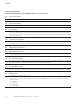
The figure below shows a block diagram of the SVX9000/
SPX9000 drive. The SVX9000/SPX9000 physically consists of
two sections, the power unit and the control unit. The
three-phase AC Choke with the DC Link Capacitor form a
LC filter, which together with the Rectifier produce the
DC voltage for the IGBT Inverter block. The AC Choke
smooths the disturbances from the utility into the SVX9000/
SPX9000 as well as the high frequency disturbances caused
by the SVX9000/SPX9000 on the utility line. It also improves
the input current waveform to the SVX9000/SPX9000. The
IGBT Inverter produces a symmetrical three-phase pulse
width modulated adjustable frequency AC voltage to the
motor.
The Motor and Application Control block contains a
microprocessor with customized software. The
microprocessor controls the motor based on Measured
Signals, parameter value settings, and commands from the
Control I/O Block and the Control Module. The Motor and
Application Control block commands the Motor Control
ASIC which calculates the IGBT switching positions. Gate
Drivers amplify these signals for driving the IGBT Inverter.
The Control Keypad is a link between the user and the
SVX9000/SPX9000. With the Control Keypad, the user can
set parameter values, read status information, and issue
control commands. The Control Keypad is removable and
can be mounted externally and connected with the
appropriate cable. Instead of the Control Keypad, a PC can
be used to control the SVX9000/SPX9000 by cable
connecting it where the Control Keypad is normally
connected or through an option board.
The Control I/O Block is isolated from line potential and may
be connected to or isolated from ground by the choice of the
control I/O board that is used. OPTA8 is isolated ground,
OPTA1 and OPTA9 are not.
Input and Output EMC-Filters are not required for the
functionality of the SVX9000/SPX9000. They are only needed
for compliance with the EU EMC directive as detailed in the
following section.
SVX9000/SPX9000 Block Diagram
Output
Measure-
ments
W
V
U
Motor
IGBT
Inverter
Current
Sensors
Voltage
Sensors
Utility
EMC
Rectifier
Charg Res
Brake
Chopper
3~
3~
Brake Resistor
Control
I/O
Gate
Drivers
Power
Module
Control
Module
RS-232
Control
Keypad
Power
Supply
Input
L3
L2
L1
EMC
PE
Fan
AC Choke
Motor
Control
ASIC
Motor and
Application
Control
Control
I/O
Control
I/O
Control
I/O
Control
I/O