
Service manual


CIRCUIT DESCRIPTION
4-5
November 2001
Part No. 001-7240-001
As forward power increases, the output voltage
on pin 7 decreases. U103 then turns off more which
decreases the supply voltage applied to Vbb Control of
U101. This decreases power to maintain a stable
output level. The opposite occurs if forward power
decreases.
4.5 CONTROL LOGIC AND DISPLAY
NOTE: A block diagram of the RF and logic boards is
located on page 8-8.
4.5.1 CONTROL LOGIC
The digital control logic is based on 16-bit
CMOS microprocessor U208. The operating speed is
set by 9.8304 MHz crystal Y202. A clock shift signal
is applied to Q207. This signal goes high to shift the
clock frequency slightly on channels in which the
second harmonic interferes with the receive signal.
A serial data bus formed by MSI, MSO, and
SER_CLOCK (pins 89-91) is used to transfer data to
and from three external devices. They are 16K x 8
EEPROM U150, digital potentiometer U147, and
LCD driver U501 on the keypad/display board.
Another serial port formed by pins 54 and 56 is
used to transfer programming data to and from an
external computer. This port is fed out of the trans-
ceiver on pins 3 and 4 of the accessory connector
(UDC connector). Data is transferred to DTMF
encoder U201 by another serial bus formed by TxD0
and RxD0 (pins 53 and 57). Descriptions of the U208
pins are located in Table 4-1.
4.5.2 DISPLAY ASSEMBLY DESCRIPTION
U501 on the display board is an intelligent LCD
display controller/driver. It communicates with the
microprocessor on the logic board over a serial bus
consisting of MSCK (serial clock, pin 91), MSO
(serial data, pin 89), and DISST (display strobe, pin
43) signals. U501 is set for 1/3 bias and 1/5 duty cycle
and drives an 8-character, 14-segment display at a 98
Hz frame frequency. LCD display EH1 has 128
segments that are driven by a 34-segment signal with
four common lines.
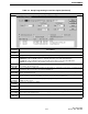
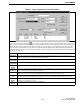
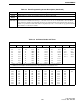
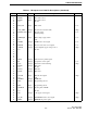
Table 4-1 Microprocessor U208 Pin Descriptions
Pin No. Port Name In/Out Descriptions Active
1 VCC - Supply voltage (L5V) -
2 OPTB Output Optional signal Low
3 CLR/CODE Output Optional encryption control signal Low
4 KEYS0 Output Key matrix scan out -
5 KEYS1 Output Key matrix scan out -
6Vss - Ground -
7 KEYS2 Output Key matrix scan out -
8 KEYS3 Output Key matrix scan out -
9 KEYS4 Output Key matrix scan out -
10 - - - -
11 - - - -
12 - - - -
13 BKLED Output LCD backlight control signal Low
14 - - - -
15 Vss - Ground -
16 - - - -
17 DISEN Output LCD driver chip enable signal -
18 - - - -
19 - - - -
20 KEYR0 Input Key matrix scan in -