
Datasheet


5
EEH210
v1.0 / Modification rights reserved
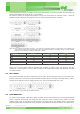
PARAMETER SYMBOL MIN TYP MAX UNITS
SPI clock cycle t
c(SPC) 100 ns
SPI clock frequency f
c(SPC) 10 MHz
CS setup time t
su(CSB) 6
ns
CS hold time t
h(CSB) 8
SDIO input setup time t
su(SI) 5
SDIO input hold time t
h(SI) 15
SDIO valid output time t
v(SO) 50
SDIO output hold time t
h(SO) 9
SDIO output disable time t
dis(SO) 50
Table 6: SPI - serial peripheral interface
Figure 7: SPI slave timing diagram
Measurement point are done at 0.3*VDD and 0.7*VDD, for both ports.
5. interFace
5.1. Pin conFiguration
Figure 8: Pin Assignment (Through View): DFN-10 3.6 x 2.8