
Datasheet


v1.0 / Modification rights reserved
4
EEH210
4.2. electrical sPeciFication
The electrical characteristics such as power consumption, low and high level input and output voltages depend on the
supply voltage. For proper communication with the sensor it is essential to make sure that signal design is strictly within
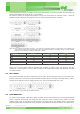
the limits given in Table 4, Table 5 and Figure 6.
PARAMETER CONDITION MIN TYP MAX UNITS
Supply Voltage VDD 2.1 3.0 3.6 V
Current Dissipation
Sleep 0.5 µA
Measuring, SEL[1:0]=00 450(TBD) µA
Average 8bit
1)
, SEL[1:0]=00 3(TBD) µA
PWM Freq. SEL[1:0]=01, 30 °C 108 120 132 Hz
Measure Freq. SEL[1:0]=01,10 2 Hz
Communication SPI and I
2
C interfaces
Table 4: DC characteristics of digital input/output pads. VCC = 3 V, T = 25 °C, unless otherwise noted.
Table 5: Timing specifications of digital input/output pads for I
2
C fast mode. Entities are displayed in Figure 4. VDD = 3V, T = 25 °C, unless
otherwise noted.
PARAMETER SYMBOL MIN TYP MAX UNITS
Output Low Voltage V
OL 0 - 0.4 V
Output High Voltage V
OH VDD X 0.7 - VDD V
Output Sink Current I
OL - - -4 mA
Input Low Voltage V
IL 0 - VDD X 0.3 V
Input High Voltage V
IH VDD X 0.7 - VDD V
SCL Frequency f
SCL 0 - 0.4 MHz
SCL High Time t
SCLH 0.6 - - μs
SCL Low Time t
SCLL 1.3 - - μs
SDA Set-Up Time t
SU 100 - - ns
SDA Hold Time t
HD 0 - 900 ns
SDA Valid Time t
VD 0 - 400 ns
SCL/SDA Fall Time t
F 20 - 300 ns
SCL/SDA Rise Time t
R
20 - 300 ns
Start condition setup time t
SUSTA 100 - - ns
Start condition hold time t
HDSTA 100 - - ns
Stop condition setup time t
SUSTO 100 - - ns
Bus free time between stop condition
and start condition
t
BUS 1.3 μs
Capacitive Load on Bus Line C
b 0 - 400 pF
Figure 6: Timing Diagram for Digital Input / Output Pads, abbreviations are explained in Table 5. SDA directions are seen from the sensor.
Bold SDA line is controlled by the sensor, plain SDA line is controlled by the micro-controller. Note that SDA valid read time is
triggered by falling edge of anterior toggle.