
User Guide


Hardware and Software Design • Manufacturing Services
P a g e 31
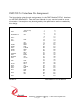
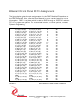
PMC PCI Pn1 Interface Pin Assignment
The figure below gives the pin assignments for the PMC Module PCI Pn1 Interface
on the PMC BiSerial-II-IO. See the User Manual for your carrier board for more
information. Unused pins may be assigned by the specification and not needed by
this design.
-12V[unused] 1 2
GND INTA# 3 4
56
BUSMODE1# +5V 7 8
910
GND - 11 12
CLK GND 13 14
GND - 15 16
+5V 17 18
AD31 19 20
AD28- AD27 21 22
AD25- GND 23 24
GND - C/BE3# 25 26
AD22- AD21 27 28
AD19 +5V 29 30
AD17 31 32
FRAME#- GND 33 34
GND IRDY# 35 36
DEVSEL# +5V 37 38
GND LOCK# 39 40
41 42
PAR GND 43 44
AD15 45 46
AD12- AD11 47 48
AD9- +5V 49 50
GND - C/BE0# 51 52
AD6- AD5 53 54
AD4 GND 55 56
AD3 57 58
AD2- AD1 59 60
+5V 61 62
GND 63 64
FIGURE 15 PMC BISERIAL-II PN1 INTERFACE