
User Guide


Hardware and Software Design • Manufacturing Services
P a g e 17
Tx load control when '1' causes a write to the channel 0 FIFO to load channels
0,1,2,3 with the same data. When '0' the FIFOs are loaded independently.
BIS2_TXs
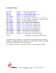
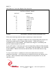
[$08] BiSerial II Txs Control Register Port read/write
CONTROL TX
DATA BIT DESCRIPTION
31-15 Spare
14-13 reference select
12 output select
11-0 divisor
FIGURE 7 PMC BISERIAL-II TX CONTROL REGISTER BIT MAP
Reference Select:
when 00 or 01 selects the oscillator = 20 MHz
when 10 the external reference is selected [IO 24]
when 11 the PCI clock is selected
The reference selected is divided using the selected divisor and then divided in half
for a 50% duty cycle reference clock. F = R/2*(D+1). Where F = the frequency
desired, R = the selected reference frequency, and D = the specified divisor. For
example to create a 5 MHz transmit frequency from the standard 20 MHz
oscillator a divide by 4 is needed. The divisor is 0x01.
The output select when '1' selects the output from the divider. When '0' the
selected reference frequency is used. If the clock programmed is not driven to
the output please check the tx clock control in the TX register.