
User Guide


Hardware and Software Design • Manufacturing Services
P a g e 11
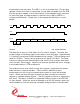
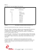
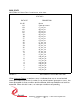
transitioned to the next value. The LSB+1 is now on the data lines. This process
repeats until the first word is transferred. If more data is available from the FIFO,
then the process repeats for the second word. In the standard timing there are
no inter-word gaps, the data stream is continuous from LSB to MSB for a
compact serial transfer. Please refer to the register bit definitions for more
details.
FIGURE 3 PS2 TIMING DIAGRAM
The data rate is set by a 12-bit field in the Txs control register. The data, and
strobe change on the falling edge and are valid on the rising edge. Approximately
1/2 period of set-up and hold are available at the receiver. The transceivers are
rated for 40 MHz. The top rate programmed for the IO is 20 MHz. The State-
machine is designed with the assumption that the PCI clock is faster than the IO
clock rate plus some margin. Faster clock rates are possible with minor changes
to the state-machine / FIFO architecture.
The receive function uses a free running shift register coupled with the receive
state-machine to capture the data. When strobe is detected to have
transitioned from low to high the state-machine starts to count the received
clocks. When the word has been received the data is moved from the shift
register to a parallel holding register. The shift register continues to capture the
next word. The data is moved from the parallel holding register to the RX FIFO
for that channel. When the strobe is detected to be low the receiver clears the
receive enable bit, sets the interrupt if enabled, and goes back to the idle state.
1/2
T
1/2
T
LSB LSB +1
...
MSB LSB
...
MSB
CLK
STB
DATA