
User Guide

Hardware and Software Design • Manufacturing Services
P a g e 10
Theory of Operation
The PMC BiSerial-II PS2 is designed for transferring data from one point to
another with a simple serial protocol.
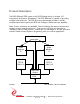
The PMC BiSerial-II PS2 features a Xilinx FPGA. The FPGA contains all of the
registers and protocol controlling elements of the BiSerial II design. Only the
transceivers, and switches are external to the Xilinx device.
The PMC BiSerial-II is a part of the PMC Module family of modular I/O products. It
meets the PMC and CMC draft Standards. In standard configuration, the PMC
BiSerial-II is a Type 1 mechanical with no components on the back of the board
and one slot wide, with 10 mm inter-board height. Contact Dynamic Engineering
for a copy of this specification. It is assumed that the reader is at least casually
familiar with this document and logic design.
The PCI interface to the host CPU is controlled by a logic block within the Xilinx.
The BiSerial II design requires one wait state for read or write cycles to any
address. The PMC BiSerial-II is capable of supporting 40 MBytes per second into
and out of the FIFO's. The wait states refer to the number of clocks after the PCI
core decode before the “terminate with data” state is reached. Two additional
clock periods account for the 1 clock delay to decode the signals from the PCI
bus and to convert the terminate with data state into the TRDY signal.
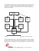
The BiSerial II can support many protocols. The PMC BiSerial-II PS2 uses serial
encoded LSB first data, clock and strobe. Data is sent in 32 bit words which are
concatenated for multiple word transfers. The timing is shown in the next
diagram.
State machines within the FPGA control all transfers between the interanal FIFO
and FPGA logic, and the FPGA and the data buffers. The TX state machine reads
from the transmit FIFOs and loads the shift registers before sending the data. The
RX state machine receives data from the data buffers and takes care of moving
data from the shift register into the RX FIFOs.
Data is read from the TX FIFOs and loaded into the shift register. The LSB is then
present at the output of the data buffer. One bit period later the data is