DYNAMIC ENGINEERING 435 Park Dr., Ben Lomond, Calif. 95005 831-336-8891 Fax 831-336-3840 sales@dyneng.com www.dyneng.com Est.
PMC BiSerial-II PS2 Bi-Directional Serial Data Interface PMC Module Dynamic Engineering 435 Park Drive Ben Lomond, CA 95005 831-336-8891 831-336-3840 FAX This document contains information of proprietary interest to Dynamic Engineering.
Table of Contents PRODUCT DESCRIPTION 6 THEORY OF OPERATION 10 ADDRESS MAP 13 PROGRAMMING 14 REGISTER DEFINITIONS 15 BIS2_BASE BIS2_TX BIS2_TXs BIS2_RX BIS2_PARDAT BIS2_STAT0 BIS2_STAT1 BIS2_COSEN BIS2_FIFOTX0-3 BIS2_FIFORX0-3 BIS2_DIR_TERM BIS2_COSEDGE 15 16 17 18 19 20 22 24 25 25 26 28 Interrupts 29 Loop-back 30 PMC PCI PN1 INTERFACE PIN ASSIGNMENT 31 PMC PCI PN2 INTERFACE PIN ASSIGNMENT 32 BISERIAL II FRONT PANEL IO PIN ASSIGNMENT 33 APPLICATIONS GUIDE 34 Interfacing 34 Hardwar
CONSTRUCTION AND RELIABILITY 35 THERMAL CONSIDERATIONS 35 WARRANTY AND REPAIR 36 SERVICE POLICY 36 OUT OF WARRANTY REPAIRS 36 FOR SERVICE CONTACT: 36 SPECIFICATIONS 37 ORDER INFORMATION 38 SCHEMATICS 38 Hardware and Software Design • Manufacturing Services P a g e 4
List of Figures FIGURE FIGURE FIGURE FIGURE FIGURE FIGURE FIGURE FIGURE FIGURE FIGURE FIGURE FIGURE FIGURE FIGURE FIGURE FIGURE FIGURE 1 2 3 4 5 6 7 8 9 10 11 12 13 14 15 16 17 PMC BISERIAL-II BLOCK DIAGRAM PMC BISERIAL-II PS2 BLOCK DIAGRAM PS2 TIMING DIAGRAM PMC BISERIAL-II PS2 INTERNAL ADDRESS MAP PMC BISERIAL-II BASE CONTROL REGISTER BIT MAP PMC BISERIAL-II INTERRUPT ENABLE REGISTER BIT MAP PMC BISERIAL-II TX CONTROL REGISTER BIT MAP PMC BISERIAL-II RX CONTROL REGISTER BIT MAP PMC BISERIAL-II PARALLEL
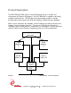
Product Description The PMC BiSerial-II PS2 is part of the PMC Module family of modular I/O components by Dynamic Engineering. The PMC BiSerial-II is capable of providing multiple serial protocols. The PS2 protocol implemented provides 4 serially encoded inputs and outputs plus 8 IO with Change of State interrupt capability. Other custom interfaces are available. We will redesign the state machines and create a custom interface protocol.
The standard configuration shown in Figure one makes use of two external [to the Xilinx ] FIFOs. The FIFOs can be as large as 128K deep x 32 bits wide. Some designs do not require so much memory and are more efficiently implemented using the internal FIFOs.
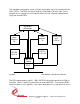
ports then the 4 FIFOs can be filled with the same pattern at the same time. Fewer PCI cycles are required and less processing by the host. The transmit data rate can be derived from the 20 MHz on-board oscillator. The normal transmitter data rate is 5 MHz (divide-by 4), other divisors are also provided. The first COS port can be used as an alternate clock source as well as the PCI clock. The max clock rate after division is required to be 20 MHz. The receiver automatically adjusts to data rates.
The serial channels are each supported by a 128 by 32-bit FIFO. The FIFOs support long word reads and writes. A full 32-bit path exists for loop-back testing of each FIFO. Data is latched and the bus immediately released on a write-cycle. On a read cycle the data is read after the bus is released from the previous read. This has the effect of adding one extra read to start capturing data, but means there is no delay in future reads. The serial format for transmit and receive is 32 bits per word, LSB first.
Theory of Operation The PMC BiSerial-II PS2 is designed for transferring data from one point to another with a simple serial protocol. The PMC BiSerial-II PS2 features a Xilinx FPGA. The FPGA contains all of the registers and protocol controlling elements of the BiSerial II design. Only the transceivers, and switches are external to the Xilinx device. The PMC BiSerial-II is a part of the PMC Module family of modular I/O products. It meets the PMC and CMC draft Standards.
transitioned to the next value. The LSB+1 is now on the data lines. This process repeats until the first word is transferred. If more data is available from the FIFO, then the process repeats for the second word. In the standard timing there are no inter-word gaps, the data stream is continuous from LSB to MSB for a compact serial transfer. Please refer to the register bit definitions for more details. CLK STB DATA LSB 1/2 T FIGURE 3 LSB +1 ... MSB LSB ...
If the receiver is enabled and a transmission is already in progress, the receiver will ignore the data until the strobe has been detected to be low then asserted high again. The design will help to make sure that the hardware stays on 32 bit data boundaries. If the FIFO is full when the receiver is enabled the state-machine will wait in the idle state until the FIFO is not full before starting a new reception.
Address Map BIS2_BASE BIS2_TX BIS2_TXS BIS2_RX BIS2_PARDAT BIS2_STAT0 BIS2_STAT1 BIS2_COSEN BIS2_FIFORX0 BIS2_FIFORX1 BIS2_FIFOTX0 BIS2_FIFOTX1 BIS2_FIFOTX2 BIS2_FIFOTX3 BIS2_DIR_TERM BIS2_FIFORX2 BIS2_FIFORX3 BIS2_COSEDGE FIGURE 4 0x0000 // 0 base control register offset 0x0004 // 1 tx control register offset 0x0008 // 2 tx special control register offset 0x000c // 3 rx control register offset 0x0010 // 4 parallel data out register 0x0014 // 5 status register 0 interrupts tx, rx, rising, falling 0x0018 //
Programming Programming the PMC BiSerial-II PS2 requires only the ability to read and write data from the host. The base address is determined during system configuration of the PCI bus. The base address refers to the first user address for the slot in which the PMC is installed. Depending on the software environment it may be necessary to set-up the system software with the PMC BiSerial-II "registration" data.
Register Definitions BIS2_BASE [$00] BiSerial II Base Control Register Port read/write CONTROL BASE DATA BIT 31-9 8 7-5 4 3 2 1 0 FIGURE 5 DESCRIPTION Spare Reset FIFO RX spare Reset FIFO TX spare spare Interrupt Set Interrupt Enable Master PMC BISERIAL-II BASE CONTROL REGISTER BIT MAP All bits are active high and are reset on power-up or reset command. Interrupt Enable Master when '1' allows interrupts generated by the PMC-BiSerial-II-PS2 to be driven onto the backplane [INTA].
BIS2_TX [$04] BiSerial II Transmitter Register Port read/write CONTROL INTERRUPT ENABLE DATA BIT 31-11 10 9 8 7 6 5 4 3 2 1 0 FIGURE 6 DESCRIPTION Spare tx load control tx clock control spare int_en_tx3 int_en_tx2 int_en_tx1 int_en_tx0 start_tx3 start_tx2 start_tx1 start_tx0 PMC BISERIAL-II INTERRUPT ENABLE REGISTER BIT MAP All bits are active high and are reset on power-up or reset command.
Tx load control when '1' causes a write to the channel 0 FIFO to load channels 0,1,2,3 with the same data. When '0' the FIFOs are loaded independently.
BIS2_RX [$0C] BiSerial II Rx Control Register Port read/write CONTROL RX DATA BIT 31-12 11 10 9 8 7 6 5 4 3 2 1 0 FIGURE 8 DESCRIPTION Spare loop_back3 loop_back2 loop_back1 loop_back0 int_en_rx3 int_en_rx2 int_en_rx1 int_en_rx0 start_rx3 start_rx2 start_rx1 start_rx0 PMC BISERIAL-II RX CONTROL REGISTER BIT MAP Start_rx0-3 when '1' enables the receiver state machine to receive messages. If Start_rx0-3 is set to a zero the reception will stop after the current word is stored in the FIFO.
BIS2_PARDAT [$10] BiSerial II Parallel Data Output Register read/write CONTROL UART DATA BIT 31-8 7-0 FIGURE 9 DESCRIPTION Spare parallel output data PMC BISERIAL-II PARALLEL OUTPUT DATA BIT MAP There are 8 potential output bits in the parallel port. The Direction and Termination register sets the direction of the bits. When the direction is set to output the bit definitions from this register are driven onto the corresponding parallel port lines. This port is direct read-write of the register.
BIS2_STAT0 [$14] BiSerial II Status Port 0 read status, write clear STATUS 0 DATA BIT 31-25 24 23 22 21 20 19 18 17 16 15 14 13 12 11 10 9 8 7 6 5 4 3 2 1 0 FIGURE 10 DESCRIPTION Spare interrupt status f7_intr_lat f6_intr_lat f5_intr_lat f4_intr_lat f3_intr_lat f2_intr_lat f1_intr_lat f0_intr_lat r7_intr_lat r6_intr_lat r5_intr_lat r4_intr_lat r3_intr_lat r2_intr_lat r1_intr_lat r0_intr_lat rx3_intr_lat rx2_intr_lat rx1_intr_lat rx0_intr_lat tx3_intr_lat tx2_intr_lat tx1_intr_lat tx0_intr_lat PMC BISERIA
The interrupt conditions are latched and held in special interrupt status latches. The latched signals are made available on the Bis2_stat0 port. The latched bits remain set until the corresponding bit is written back to the port. When an interrupt occurs or if polling is used this port can be used to determine which channel requires attention. The active channel should be taken care of and then the bit set to clear the request. The combination of port access and bit position set is used to clear the bit.
BIS2_STAT1 [$18] BiSerial II Status Port 1 read only FIFO Status, Parallel Data In & Switch Register DATA BIT 31-24 23 22 21 20 19 18 17 16 15 14 13 12 11 10 9 8 7-0 FIGURE 11 DESCRIPTION sw7-0 rx_fifo_full3 rx_fifo_full2 rx_fifo_full1 rx_fifo_full0 rx_fifo_mt3 rx_fifo_mt2 rx_fifo_mt1 rx_fifo_mt0 tx_fifo_full3 tx_fifo_full2 tx_fifo_full1 tx_fifo_full0 tx_fifo_mt3 tx_fifo_mt2 tx_fifo_mt1 tx_fifo_mt0 dat_in7-0 PMC BISERIAL-II STATUS 1 BIT MAP The Switch Read Port has the user bits.
is stored in the FIFO the status will be '0'. Tx_fifo_full3-0 is '1' when the Transmit FIFO is full for that channel. When there is less than a full FIFO the status will be '0'. Rx_fifo_mt3-0 is '1' when the Receive FIFO is empty for that channel. When data is stored in the FIFO the status will be '0'. Rx_fifo_full3-0 is '1' when the Receive FIFO is full for that channel. When there is less than a full FIFO the status will be '0'. Dat_in is the parallel data read from the parallel port.
BIS2_COSEN [$1C] BiSerial II Parallel Enable COS register Parallel Enable Change of State Register DATA BIT 31-24 23-16 15-8 7-0 FIGURE 12 DESCRIPTION spare par_int_en_f par_int_en_r par_en7-0 PMC BISERIAL-II COSEN REGISTER BIT MAP Par_en bits 7-0 correspond to the parallel IO port bits. When set the COS function is enabled for that input bit. Normally the par_en bit will not be enabled for ports defined to be outputs.
BIS2_FIFOTX0-3 [$28,2C,30,34] BiSerial II Tx FIFO write-read port The BiSerial II supports 32-bit writes to the transmit data FIFO. Data is aligned D31-0. Normally this port is only written to, but for loop-back testing the contents of the FIFO can be read out over the PCI bus. The data is moved from the FIFO to the holding register at the end of a read cycle.
BIS2_DIR_TERM [$38] BiSerial II Direction and Termination Register Port read/write CONTROL DIR_TERM REGISTER DATA BIT 13-0 29-16 FIGURE 13 DESCRIPTION DIRection TERMination 13-0 13-0 0 = read 1 = drive 1 = terminated PMC BISERIAL-II DIRECTION TERMINATION CONTROL BIT MAP The direction for each of the 32 differential pairs is controlled through this port. The port defaults to zero, which corresponds to tri-stating the drivers and no terminations enabled.
The terminations for the receive groups should be set to terminate with the user software in most cases. [term_9 - term_11] If the Parallel Port is set to be an input with the direction bits then the corresponding termination bits should also be set. CONTROL TERM_0..7 TERM_8 TERM_9 TERM_10 TERM_11 TERM_12 TERM_13 CORRESPONDING IO BIT(S) IO_0..7 IO_8..11 IO_12..15 IO_16..19 IO_20..23 IO_24..27 IO_28..
BIS2_COSEDGE [$44] BiSerial II COS Edge Definition Register Change of State Edge Register DATA BIT 31-16 15-8 7-0 FIGURE 14 DESCRIPTION Spare falling7-0 rising7-0 PMC BISERIAL-II COSEDGE REGISTER BIT MAP Rising when set for a channel enables that COS state-machine [if enabled] to look for rising edge transitions and to set the status bit when found. Falling when set for a channel enables that COS state-machine [if enabled] to look for falling edge transitions and to set the status bit when found.
Interrupts PMC BiSerial-II interrupts are treated as auto-vectored. When the software enters into an exception handler to deal with a PMC BiSerial-II interrupt the software must read the status register to determine the cause(s) of the interrupt, clear the interrupt request(s) and process accordingly. Power on initialization will provide a cleared interrupt request and interrupts disabled.
Loop-back The Engineering kit has reference software, which includes an external loop-back test. The PS2 version of the PMC-BiSerial II utilizes a 68 pin SCSI II front panel connector. The test requires an external cable with the following pins connected.
PMC PCI Pn1 Interface Pin Assignment The figure below gives the pin assignments for the PMC Module PCI Pn1 Interface on the PMC BiSerial-II-IO. See the User Manual for your carrier board for more information. Unused pins may be assigned by the specification and not needed by this design.
PMC PCI Pn2 Interface Pin Assignment The figure below gives the pin assignments for the PMC Module PCI Pn2 Interface on the PMC BiSerial-II-IO. See the User Manual for your carrier board for more information. Unused pins may be assigned by the specification and not needed by this design.
BiSerial II Front Panel IO Pin Assignment The figure below gives the pin assignments for the PMC Module IO Interface on the PMC BiSerial-II. Also, see the User Manual for your carrier board for more information. GND* is a plane which is tied to GND through a 1206 0Ω resistor. DC, AC or open are options. For customized version, or other options, contact Dynamic Engineering.
Applications Guide Interfacing The pin-out tables are displayed with the pins in the same relative order as the actual connectors. The pin definitions are defined with noise immunity in mind. The pairs are chosen to match standard SCSI II/III cable pairing to allow a low cost commercial cable to be used for the interface. Some general interfacing guidelines are presented below. Do not hesitate to contact the factory if you need more assistance. Watch the system grounds.
Construction and Reliability PMC Modules were conceived and engineered for rugged industrial environments. The PMC BiSerial-II is constructed out of 0.062 inch thick FR4 material. Through hole and surface mounting of components are used. IC sockets use screw machine pins. High insertion and removal forces are required, which assists in the retention of components.
Warranty and Repair Please refer to the warranty page on our website for the current warranty offered and options. http://www.dyneng.com/warranty.html Service Policy Before returning a product for repair, verify as well as possible that the suspected unit is at fault. Then call the Customer Service Department for a RETURN MATERIAL AUTHORIZATION (RMA) number.
Specifications Host Interface: [PMC] PCI Mezzanine Card - 32 bit Serial Interface: 4 Tx and 4 Rx serial interfaces each with Data, Clock, Stb. 32 bit word size, LSB first, multiple words Tx Data rates generated: 20 MHz oscillator, PCI clock or external clock references with programmable 12 bit divider for programmable frequencies. Max transmit and receive rate of 20 MHz with current VHDL. Custom oscillators can be installed for alternate frequencies. Rx Data rates accepted: Continuous up to 20 MHz.
Order Information PMC BiSerial-II PS2 PMC Module with 4 TX serial channels, 4 Rx serial channels, 8 bit parallel port with COS interrupt capability. RS-485 IO. 32 bit data interface Eng Kit–PMC BiSerial-II HDEterm68 - 68 position screw terminal adapter http://www.dyneng.com/HDEterm68.html HDEcabl68 - 68 IO twisted pair cable http://www.dyneng.com/HDEcabl68.html Technical Documentation, 1. PMC BiSerial-II Schematic 2.