DYNAMIC ENGINEERING 435 Park Dr., Ben Lomond, Calif. 95005 831-336-8891 Fax 831-336-3840 sales@dyneng.com www.dyneng.com Est.
PMC-4U Quad UART - Dual Synchronous Serial Data Interface PMC Module This document contains information of proprietary interest to Dynamic Engineering. It has been supplied in confidence and the recipient, by accepting this material, agrees that the subject matter will not be copied or reproduced, in whole or in part, nor its contents revealed in any manner or to any person except to meet the purpose for which it was delivered.
Table of Contents PRODUCT DESCRIPTION 6 THEORY OF OPERATION 9 ADDRESS MAP 10 PROGRAMMING 12 REGISTER DEFINITIONS 13 PMC4U_BASE PMC4U_STAT PMC4U_MSK PMC4U_SCC_IVEC PMC4U_DIR_TERM PMC4U_SW_IN PMC4U_SCC_A_CNTL PMC4U_SCC_A_DATA PMC4U_SCC_B_CNTL PMC4U_SCC_B_DATA PMC4U_UART_A PMC4U_UART_B PMC4U_UART_C PMC4U_UART_D PMC4U_IRUPT/PMC4U_IRUPT_CLR 13 16 16 17 17 18 19 19 19 19 20 20 20 20 21 Interrupts 22 Loop-back 23 PMC PCI PN1 INTERFACE PIN ASSIGNMENT 24 PMC PCI PN2 INTERFACE PIN ASSIGNMENT 25 PM
Interfacing 28 CONSTRUCTION AND RELIABILITY 29 THERMAL CONSIDERATIONS 29 WARRANTY AND REPAIR 30 SERVICE POLICY 31 OUT OF WARRANTY REPAIRS 31 FOR SERVICE CONTACT: 31 SPECIFICATIONS 32 ORDER INFORMATION 33 SCHEMATICS 33 Hardware and Software Design • Manufacturing Services P a g e 4
List of Figures FIGURE 1 FIGURE 2 FIGURE 3 FIGURE 4 FIGURE 5 FIGURE 6 FIGURE 7 FIGURE 8 FIGURE 9 FIGURE 10 FIGURE 11 FIGURE 12 FIGURE 13 PMC-4U BLOCK DIAGRAM PMC-4U INTERNAL ADDRESS MAP PMC-4U UART ADDRESS MAP PMC-4U BASE CONTROL REGISTER BIT MAP PMC-4U TX CONTROL REGISTER BIT MAP PMC-4U INTERRUPT MASK REGISTER BIT MAP PMC-4U DIRECTION TERMINATION CONTROL BIT MAP PMC-4U SWITCH READ BIT MAP PMC-4U INTERRUPT STATUS/CLEAR PMC-4U PN1 INTERFACE PMC-4U PN2 INTERFACE PMC-4U FRONT PANEL INTERFACE PMC-4U PN4 INTERF
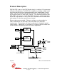
Product Description PMC-4U-CACI is part of the PMC Module family of modular I/O components by Dynamic Engineering. The PMC-4U is capable of providing multiple serial protocols both synchronous and asynchronous with a wide range of baud rates. The CACI interface uses an RS-423 driver, an RS-422 driver, and an RS-422 receiver for each UART channel.
An EXAR XR16C854 implements the UART interface. This quad UART device is compatible with the industry standard 16550 UART, but is equipped with 128 byte FIFOs, independent Tx and Rx FIFO counters, automatic hardware/software flow control, and many other enhanced features. An 18.432 MHz oscillator supplies the reference clock for this device allowing baud rates up to 1.152 Mbps. The synchronous interface uses a Zilog Serial Communication Controller, the Z85C30.
There is also a master interrupt enable that can be set to gate the interrupt onto the PCI bus. The interrupt status is still available in a status register even when the master interrupt enable is off. This facilitates polled operation of interrupt conditions. The individual interrupt conditions are specified in the internal registers of the UART and SCC. Please see the XR16C854 and Z85C30 documentation for more information on interrupt conditions and configuration.
Theory of Operation The PMC-4U is designed for transferring data from one point to another with a variety of serial protocols. The PMC-4U features a Xilinx FPGA. The FPGA contains the general control and status registers as well as the interface to the quad UART, SCC, and IO drivers and receivers. Many additional control and status registers reside in the UART and SCC, which are accessed through the Xilinx interface. The PMC-4U is a part of the PMC Module family of modular I/O products.
Address Map REGISTER PMC4U_BASE PMC4U_STAT PMC4U_MSK PMC4U_SCC_IVEC PMC4U_DIR_TERM PMC4U_SW_IN PMC4U_SCC_A_CNTL PMC4U_SCC_A_DATA PMC4U_SCC_B_CNTL PMC4U_SCC_B_DATA PMC4U_UART_A PMC4U_UART_B PMC4U_UART_C PMC4U_UART_D PMC4U_IRUPT PMC4U_IRUPT_CLR FIGURE 2 OFFSET FUNCTION 0X00 0X04 0X08 0X0C 0X10 0X14 0X18 0X1C 0X20 0X24 0X40 0X60 0X80 0XA0 0XE0 0XE0 TYPE base control status read interrupt mask control SCC interrupt vector read direction and termination control read user switch SCC channel A control SCC chann
REGISTER OFFSET FUNCTION PMC4U_UART_DATA 0X00 UART read/write data PMC4U_UART_IEN 0X04 UART write interrupt enable PMC4U_UART_ISTAT 0X08 UART read interrupt status PMC4U_UART_FCNTL 0X08 UART write FIFO control PMC4U_UART_LCNTL 0X0C UART write line control PMC4U_UART_MCNTL 0X10 UART write modem control PMC4U_UART_LSTAT 0X14 UART read line status PMC4U_UART_MSTAT 0X18 UART read modem status PMC4U_UART_SPAD 0X1C UART read/write scratchpad UART baud rate register defines (enabled when *LCNTL bit-7 = 1) PMC4U
Programming Programming the PMC-4U requires only the ability to read and write data from the host. The base address is determined by the PMC Carrier board. The base address refers to the first user address for the slot in which the PMC is installed. Depending on the software environment it may be necessary to set-up the system software with the PMC-4U "registration" data. For example in WindowsNT there is a system registry, which is used to identify the resident hardware. The PMC-4U VendorId = 0x10EE.
Register Definitions PMC4U_BASE [0X00] PMC-4U Control Register Port read/write CONTROL BASE DATA BIT DESCRIPTION 31-22 21-20 19 18 17 16 15-0 spare test mode select master interrupt enable force interrupt SCC reset UART reset spare FIGURE 4 PMC-4U BASE CONTROL REGISTER BIT MAP All bits are active high and are reset on power-up or reset command. Test mode select is used to enable different drivers and receivers to allow thorough testing of the IO circuitry.
SCC SCC SCC SCC Tx A Rx A Rx Clk RTS A SCC Tx B SCC Rx B OUT_4 (188) AUX_IN_0 (enhanced hysteresis 188) AUX_IN_1 (enhanced hysteresis 188) AUX_OUT_0 (open drain) IO_15 (RS422) IO_13 (RS422) When test mode select is “10” the following changes are made (if a signal is not listed here, its connection remains the same): Signal Function Driver/Receiver UART Rx A IO_1 (RS422) UART Rx B IO_3 (RS422) UART Rx C IO_5 (RS422) UART Rx D IO_7 (RS422) SCC RTS A AUX_OUT_1 (open drain) SCC Tx B SCC Rx B IO
UART Tx C UART Rx C OUT_6 (RS423) IN_6 (RS232) UART Tx D UART Rx D OUT_7 (RS423) IN_7 (RS232) Master interrupt enable when ‘1’ gates all interrupts through to the PCI host. When ‘0’ the interrupts can be used for status without interrupting the host. Force interrupt is used for test and software development purposes to create an interrupt request. 1 = assert interrupt request. 0 = normal operation. Useful to stimulate interrupt acknowledge routines for development.
PMC4U_STAT [0X04] PMC-4U Status Port read only STATUS DATA BIT 31-2 1 0 DESCRIPTION spare interrupt out interrupt status FIGURE 5 PMC-4U TX CONTROL REGISTER BIT MAP Interrupt out indicates that an interrupt is asserted on the PCI bus. Interrupt status indicates that an interrupt condition exists, however if the master interrupt enable is not asserted, then the interrupt will not be asserted on the PCI bus. This bit can be used to operate the card in polled mode without interrupting the host.
PMC4U_SCC_IVEC [0X0C] PMC-4U SCC Interrupt Acknowledge/Vector Read A read from this address causes the SCC interrupt acknowledge signal to be asserted. If an interrupt condition exists in the SCC, it will respond by placing an interrupt vector on the local data bus. This vector is specified by the user and, depending on the state set in the SCC registers, may contain status information about the cause of the interrupt.
Parallel termination resistors are supplied on each differential pair along with a switch to allow the user to select which lines are terminated and where. In some systems it will make sense to terminate the lines in the cable and in others it will make sense to use the onboard terminations. CONTROL TERM0 TERM1 TERM2 TERM3 CORRESPONDING IO BITS IO_0..7 IO_8..11 IO_12..13 IO_14..
PMC4U_SCC_A_CNTL [0X18] PMC-4U SCC Channel A Control Register read/write This address is used to access all of the channel A registers. In order to access a register other than this base register, the register number is first written to this address. A subsequent read or write will read from or write to the desired register. After this process is completed, the pointers are reset so that the base register is once again accessed. See the Z85C30 documentation for more information on this process.
PMC4U_UART_A [0X40] PMC-4U UART A Base Address This is the base address for the eight register addresses associated with UART A. Figure 3 gives an overview of these registers and their functions. For more details on the access and functions of these registers see the XR16C854 documentation. PMC4U_UART_B [0X60] PMC-4U UART B Base Address This is the base address for the eight register addresses associated with UART B. Figure 3 gives an overview of these registers and their functions.
PMC4U_IRUPT/PMC4U_IRUPT_CLR [0XE0] PMC-4U Interrupt Latch read status/write clear INTERRUPT STATUS DATA BIT 4 3 2 1 0 FIGURE 9 DESCRIPTION SCC interrupt UART D interrupt UART C interrupt UART B interrupt UART A interrupt PMC-4U INTERRUPT STATUS/CLEAR The bits in this register indicate that an interrupt has been received from the corresponding device. These bits are latched and once set will remain set until a one is written to the bit to be cleared.
Interrupts PMC-4U interrupts are treated as auto-vectored. When the software enters into an exception handler to deal with a PMC-4U interrupt the software must read the interrupt register to determine the cause(s) of the interrupt, change the interrupt mask, process accordingly to clear the interrupt condition, and then clear the associated bit in the interrupt register.
Loop-back The Engineering kit has reference software, which includes external loopback tests for the SCC and the UART. These tests require an external cable with the following pins connected.
PMC PCI Pn1 Interface Pin Assignment The figure below gives the pin assignments for the PMC Module PCI Pn1 Interface on the PMC-4U-IO. See the User Manual for your carrier board for more information. Unused pins may be assigned by the specification and not needed by this design.
PMC PCI Pn2 Interface Pin Assignment The figure below gives the pin assignments for the PMC Module PCI Pn2 Interface on the PMC-4U-IO. See the User Manual for your carrier board for more information. Unused pins may be assigned by the specification and not needed by this design.
PMC-4U Front Panel IO Pin Assignment The figure below gives the pin assignments for the PMC Module IO Interface on the PMC-4U. Also, see the User Manual for your carrier board for more information. GND* is a plane which is tied to GND through a 1206 0Ω resistor. AC or open are options – contact Dynamic Engineering.
PMC Pn4 User Interface Pin Assignment The figure provides the pin assignments for the PMC-4U Module routed to Pn4. Also, see the User Manual for your carrier board for more information. GND IO_0+ (UART Rx A) IO_1+ IO_2+ (UART Rx B) IO_3+ IO_4+ (UART Rx C) IO_5+ IO_6+ (UART Rx D) IO_7+ GND IO_8+ (UART Tx A) IO_9+ (UART Tx B) IO_10+ (UART Tx C) IO_11+ (UART Tx D) IO_12+ IO_13+ (SCC Rx B) IO_14+ IO_15+ (SCC Tx B) GND IN_0 IN_1 IN_2 IN_3 IN_4 IN_5 IN_6 IN_7 GND AUX_IN_0 (SCC Rx A) AUX_IN_1 (SCC Rx Clk) GND +3.
Applications Guide Interfacing The pin-out tables are displayed with the pins in the same relative order as the actual connectors. The pin definitions are defined with noise immunity in mind. The pairs are chosen to match standard SCSI II/III cable pairing to allow a low cost commercial cable to be used for the interface. Some general interfacing guidelines are presented below. Do not hesitate to contact the factory if you need more assistance. Watch the system grounds.
Construction and Reliability PMC Modules were conceived and engineered for rugged industrial environments. The PMC-4U is constructed out of 0.062 inch thick FR4 material. Through hole and surface mounting of components are used. IC sockets use gold plated screw machine pins. High insertion and removal forces are required, which assists in the retention of components.
Warranty and Repair Dynamic Engineering warrants this product to be free from defects in workmanship and materials under normal use and service and in its original, unmodified condition, for a period of one year from the time of purchase. If the product is found to be defective within the terms of this warranty, Dynamic Engineering's sole responsibility shall be to repair, or at Dynamic Engineering's sole option to replace, the defective product.
Service Policy Before returning a product for repair, verify as well as possible that the suspected unit is at fault. Then call the Customer Service Department for a RETURN MATERIAL AUTHORIZATION (RMA) number. Carefully package the unit, in the original shipping carton if this is available, and ship prepaid and insured with the RMA number clearly written on the outside of the package. Include a return address and the telephone number of a technical contact.
Specifications Host Interface: PCI Mezzanine Card Serial Interfaces: Four UART channels each with an RS422 driver and receiver and an RS423 driver. One synchronous channel with Mil. Std. 188114A Type 1 enhanced hysteresis receivers for clock and data, a 188 driver for Tx data, and an open drain PTT interface on the RTS line. Another synchronous channel with RS422 driver and receiver. TX Data rates generated: Up to 1.152 MHz for the UART channels. Up to 3.072 MHz for the SCC in synchronous mode.
Order Information PMC-4U PMC Module with 4 UART channels and 2 synchronous/asynchronous serial channels Programmable baud rates differential and single ended data inputs and outputs RS-188, 232, 422, 423, 485 standards supported 32 bit data interface Eng Kit–PMC-4U HDEterm68 - 68 position screw terminal adapter HDEcabl68 - 68 IO twisted pair cable Technical Documentation, 1. PMC-4U Schematic 2.