
Data Sheet

Version 2.2
DHAN-T DECT-ULE Module
Supplementary Info
April 16, 2020
DSP Group Confidential
13/17
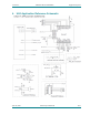
6. Application PCB Design Recommendations
It is recommended that unused pads on the Application PCB not be left as isolated islands of copper but rather
be anchored with via to inner layers of the PCB. It is also recommend that GND vias be applied liberally in the
vicinity of GND pins 1, 21, 36 and 56.
The following layout recommendations for embedding the DHAN-T on the Application Board:
1. Implement a solid ground under the DHAN-T module
2. Do not route signal traces under the module. Use the bottom layer for signal routing
3. Locate the antenna on the edge of the PCB
4. Release from GND on all layers under the DHAN-T antenna