
User's Manual
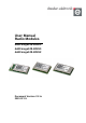
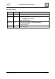
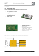


Table Of Contents
- 1. Overview
- 2. Applications
- 3. Features
- 4. Technical data
- 5. Mechanical size
- 6. Soldering profile
- 7. Pin assignment
- 8. PCB design
- 9. Clock
- 10. Application circuits
- 11. Programming
- 12. Pre-flashed firmware
- 13. Adapter boards
- 14. Radio certification
- 15. Ordering information
- 16. Packaging dimension
- 17. Revision notes
- 18. References

User Manual
Version 1.1c
2013-07-01
OEM radio modules deRFmega
www.dresden-elektronik.de
Page 8 of 52
3.2. deRFmega128-22M10
The radio module deRFmega128-22M10 offers the following features:
Tiny size: 19.0 x 13.2 x 3.0 mm
55 LGA pads 0.6 x 0.6 mm
Supply voltage 1.8 V to 3.6 V
RF shielding
Onboard 32.768 kHz crystal
(Deep-Sleep clock) and
16 MHz crystal
Application interfaces:
2x UART, 1x TWI, 1x ADC
GPIO interface
Debug/Programming interfaces:
1x SPI, 1x JTAG, 1x ISP
Solderable 2.4 GHz RF output pads
(1x RFOUT, 3x RFGND)
Certification: CE, FCC pending
Figure 2 shows the block diagram of the radio module deRFmega128-22M10.
ATmega128RFA1
Transceiver crystal
16MHz [+/-10ppm]
JTAG
UART
VCC
1.8V to 3.6V
Watch crystal
32.768kHz
SPI
TWI
ADC
GPIO
RFout
Figure 2: Block diagram deRFmega128-22M10