
User's Manual


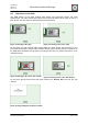
Table Of Contents
- 1. Overview
- 2. Applications
- 3. Features
- 4. Technical data
- 5. Mechanical size
- 6. Soldering profile
- 7. Pin assignment
- 8. PCB design
- 9. Clock
- 10. Application circuits
- 11. Programming
- 12. Pre-flashed firmware
- 13. Adapter boards
- 14. Radio certification
- 15. Ordering information
- 16. Packaging dimension
- 17. Revision notes
- 18. References

User Manual
Version 1.1c
2013-07-01
OEM radio modules deRFmega
www.dresden-elektronik.de
Page 39 of 52
8.5. Traces
Common signal traces should be designed with these guidelines:
Traces on top layer are not allowed under the module (see Figure 29)
Traces on mid layers and bottom layers are allowed (see Figure 29)
Route traces straight away from module (see Figure 26)
Do not use heat traps of components directly on the RF trace
Do not use 90 degree corners. Better is 45 degree or rounded corners.
The trace design for RF signals has a lot of more important points to regard. It defines the
trace impedance and therefore the signal reflection and transmission. The most commonly
used RF trace designs are Microstrip and Grounded Coplanar Wave Guide (GCPW). The
dimension of the trace is depending on the used PCB material, the height of the material to
the next ground plane, a PCB with or without a ground plane, the trace width and for GCPW
the gap to the top ground plane. The calculation is not trivial, therefore specific literature and
web content is available (see [2])
The reference plane to the GCPW should always be a ground area, that means the bottom
layer for a 2 layer design and mid layer 1 for a 4 layer design (see Figure 30). Furthermore,
it is important to use a PCB material with a known layer stack and relative permittivity. Small
differences in the material thickness have a great influence on the trace impedance,
especially on 4 layer designs.
Top
Bottom
Mid 1
Mid 2
2 Layer 4 Layer
h
g g
w
g g
w
h
FR4 ≈ 4.3
FR4 ≈ 4.3
Figure 30: GCPW trace design