
User's Manual


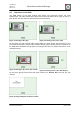
Table Of Contents
- 1. Overview
- 2. Applications
- 3. Features
- 4. Technical data
- 5. Mechanical size
- 6. Soldering profile
- 7. Pin assignment
- 8. PCB design
- 9. Clock
- 10. Application circuits
- 11. Programming
- 12. Pre-flashed firmware
- 13. Adapter boards
- 14. Radio certification
- 15. Ordering information
- 16. Packaging dimension
- 17. Revision notes
- 18. References

User Manual
Version 1.1c
2013-07-01
OEM radio modules deRFmega
www.dresden-elektronik.de
Page 38 of 52
8.4. Layers
The use of 2 or 4 layer boards have advantages and disadvantages for the design of a
custom base board.
Table 8-1: 2 and 4 layer board properties in comparison
2 Layer board
4 Layer board
(-) only 2 layers available for routing the traces
and design a proper ground area
(+) 4 layers available for routing the traces
and design a proper ground area
(-) only 1 layer available for routing the traces
under the module
(+) 3 layers available for routing the traces
under the module
(-) no separate VCC plane usable
(+) separate VCC plane usable
(+) cheaper than 4 layers
(-) more expensive than 2 layers
Top
Bottom
Mid 1
Mid 2
2 Layer 4 Layer
Module
4 Layer
Traces under
module:
Not allowed
allowed
allowed
allowed
Traces under
module:
Not allowed
allowed
Figure 29: Layer design of 2 and 4 layer boards