
User's Manual


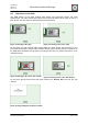
Table Of Contents
- 1. Overview
- 2. Applications
- 3. Features
- 4. Technical data
- 5. Mechanical size
- 6. Soldering profile
- 7. Pin assignment
- 8. PCB design
- 9. Clock
- 10. Application circuits
- 11. Programming
- 12. Pre-flashed firmware
- 13. Adapter boards
- 14. Radio certification
- 15. Ordering information
- 16. Packaging dimension
- 17. Revision notes
- 18. References

User Manual
Version 1.1c
2013-07-01
OEM radio modules deRFmega
www.dresden-elektronik.de
Page 37 of 52
8.2.3. Footprint of deRFmega128-22M12
Figure 28 shows an exemplary base board footprint for deRFmega128-22M12. Only the top
layer (red) is visible. The mid and bottom layers are hidden. The pad copper area (red, not
visible) and the paste dimension (grey) have the same size of 0.6 x 0.6 mm. The solder stop
clearance (purple) has a value of 0.1 mm.
The RF ground pads are connected to each other and to the board ground to ensure a
proper ground area. For the most applications it is not necessary to separate the RF ground
from system ground. The RF ground area in Figure 28 has a vertical dimension of 9.4 mm.
The ground vias are not plugged. In this area are no other radio module signals. An
unintentional short-circuit is therefore accepted. Do not place copper on any other area
among the entire module. Solder stop could be used everywhere.
The RF trace design depends on the used base board and is described detailed Section 8.5.
Figure 28: Exemplary base board footprint for 22M12 (top view)
8.3. Ground plane
The performance of RF applications mainly depends on the ground plane design. The often
used chip ceramic antennas are very tiny, but they need a proper ground plane to establish a
good radiation pattern. Every board design is different and cannot easily be compared to
each other. Some practical notes for the ground plane design are described below:
Regard to the design guideline of the antenna manufacturer
Use closed ground planes on the PCB edges on top and bottom layer
Connect the ground planes with lots of vias. Place it inside the PCB like a chessboard
and on the edges very closely.