
User's Manual


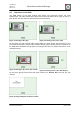
Table Of Contents
- 1. Overview
- 2. Applications
- 3. Features
- 4. Technical data
- 5. Mechanical size
- 6. Soldering profile
- 7. Pin assignment
- 8. PCB design
- 9. Clock
- 10. Application circuits
- 11. Programming
- 12. Pre-flashed firmware
- 13. Adapter boards
- 14. Radio certification
- 15. Ordering information
- 16. Packaging dimension
- 17. Revision notes
- 18. References

User Manual
Version 1.1c
2013-07-01
OEM radio modules deRFmega
www.dresden-elektronik.de
Page 34 of 52
8. PCB design
The PCB design of a radio module base board is important for a proper performance of
peripherals and the radio. The next subsections give design hints to create a custom base
board.
8.1. Technology
The described design has the main goal to use standard PCB technology to reduce the costs
and cover a wider application range.
Design parameters
150 µm manufacturing process
4 layer PCB with FR4 Prepreg
No via plugging
Via hole size: 0.2 mm
Via diameter: 0.6 mm
8.2. Base board footprint
The footprint for a custom base board depends on the radio module used. The mechanical
dimensions are shown in Section 5. The following part describes an example to design a
base board.
Properties of stencil and solder paste
Stencil = 130 µm thickness
Lead free solder paste (particle size from 20 to 38 µm)
Properties of signal pads
Signal pad dimension = 0.6 x 0.6 mm (rectangular, red)
Signal pad cut-out on stencil = 0.6 x 0.6 mm (rectangular, grey)
Clearance to solder stop = 0.1 mm (purple)
Figure 24: Signal pad footprint design
Properties of RF pads
RF ground pad dimension = 1.6 x 0.5 mm (round, red)
RF ground pad cut-out on stencil = 1.3 x 0.2 mm (round, grey)
RF signal-out pad dimension = 0.6 x 0.6 mm (round, red)
RF signal-out pad cut-out on stencil = 0.6 x 0.6 mm (round, grey)
Clearance to solder stop = 0.1 mm (purple)