
User's Manual


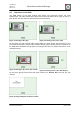
Table Of Contents
- 1. Overview
- 2. Applications
- 3. Features
- 4. Technical data
- 5. Mechanical size
- 6. Soldering profile
- 7. Pin assignment
- 8. PCB design
- 9. Clock
- 10. Application circuits
- 11. Programming
- 12. Pre-flashed firmware
- 13. Adapter boards
- 14. Radio certification
- 15. Ordering information
- 16. Packaging dimension
- 17. Revision notes
- 18. References

User Manual
Version 1.1c
2013-07-01
OEM radio modules deRFmega
www.dresden-elektronik.de
Page 31 of 52
7.3.1. Internal front-end control
The front-end of deRFmega128-22M12 has an internal PA for transmit and a LNA for receive
mode. An additionally antenna diversity feature is usable to select the antenna with the best
link budget. The front-end control includes three MCU port pins (Figure 23). They are used
to choose the TX/RX antenna, de-/activate transmit and receive mode and de-/activate the
sleep mode. Table 7-6 and Table 7-7 show the logic values. A logic ‘0’ is specified with a
voltage level of 0 V to 0.3 V. A logic ‘1’ is specified with a value of VCC - 0.3 V to 3.6 V. The
control signals DIG1, DIG3 and PD6 are available on the LGA pins.
Table 7-6: Front-end control of TX/RX and sleep mode
Mode description
PG1/DIG1
PD6/T1
PG0/DIG3
PA_ANT SEL
PA_CSD
PA_CTX
All off (sleep mode)
X
0
0
RX LNA mode
X
1
0
TX mode
X
1
1
Table 7-7: Front-end control of TX/RX antenna
Mode description
PG1/DIG1
PD6/T1
PG0/DIG3
PA_ANT SEL
PA_CSD
PA_CTX
RFOUT1 port enabled
0
X
X
RFOUT2 port enabled
1
X
X
ATmega128RFA1
Transceiver crystal
16MHz [+/-10ppm]
JTAG
UART
VCC
2.0V to 3.6V
Watch crystal
32.768kHz
SPI
TWI
ADC
GPIO
RFout 1
RFout 2
RF
DIG1
PD6
DIG3
ANT SEL
PA
LNA
TX/RX
Sleep
Figure 23: Block diagram of front-end functionality and control
Note: Do not leave any unused RFOUT pad unterminated.