
User's Manual
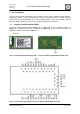
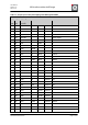
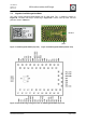


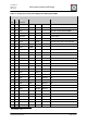
Table Of Contents
- 1. Overview
- 2. Applications
- 3. Features
- 4. Technical data
- 5. Mechanical size
- 6. Soldering profile
- 7. Pin assignment
- 8. PCB design
- 9. Clock
- 10. Application circuits
- 11. Programming
- 12. Pre-flashed firmware
- 13. Adapter boards
- 14. Radio certification
- 15. Ordering information
- 16. Packaging dimension
- 17. Revision notes
- 18. References

User Manual
Version 1.1c
2013-07-01
OEM radio modules deRFmega
www.dresden-elektronik.de
Page 30 of 52
31
-
GND
32
49
PE3
OC3A
AIN1
33
5
PE4
OC3B
INT4
34
51
PE5
OC3C
INT5
35
-
NC
Leave unconnected
36
-
NC
Leave unconnected
37
29
PD4
ICP1
38
60
AVDD
Leave unconnected if unused
(1.8V TRX Voltage Output)
39
62
AREF
40
63
PF0
ADC0
ADC
41
64
PF1
ADC1
ADC
42
1
PF2
ADC2
DIG2
ADC
43
2
PF3
ADC3
DIG4
44
-
GND
45
6
PF7
ADC7
TDI
JTAG
46
5
PF6
ADC6
TDO
JTAG
47
4
PF5
ADC5
TMS
JTAG
48
3
PF4
ADC4
TCK
JTAG
49
-
GND
50
-
VCC
2.0 V to 3.6 V
51
-
GND
52
-
RFGND
53
-
RFOUT2
50 Ω impedance*
54
-
RFGND
55
-
RFGND
56
-
RFGND
57
-
RFOUT1
50 Ω impedance*
58
-
RFGND
59
-
RFGND
Note: PG4/TOSC1 and PG3/TOSC2 are internally connected to a 32.768 kHz crystal.
*) If one of both RFOUT pads of the radio module deRFmega128-22M12 is unused, it
must be terminated with 50 ohms to ground. This action ensures the proper function
of the internal power amplifier and will reduce the power consumption.