
User's Manual
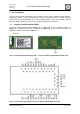
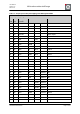
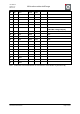
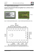


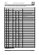
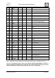
Table Of Contents
- 1. Overview
- 2. Applications
- 3. Features
- 4. Technical data
- 5. Mechanical size
- 6. Soldering profile
- 7. Pin assignment
- 8. PCB design
- 9. Clock
- 10. Application circuits
- 11. Programming
- 12. Pre-flashed firmware
- 13. Adapter boards
- 14. Radio certification
- 15. Ordering information
- 16. Packaging dimension
- 17. Revision notes
- 18. References

User Manual
Version 1.1c
2013-07-01
OEM radio modules deRFmega
www.dresden-elektronik.de
Page 24 of 52
7.2. Signals of deRFmega128-22M10
The radio module deRFmega128-22M10 has 55 LGA pads. The ‘1’ marking is shown in
Figure 18. Consider that the pin numbering in Figure 19 is shown from top view. All LGA
pads are listed in Table 7-2.
Figure 17: deRFmega128-22M10 (top view)
Figure 18: deRFmega128-22M10 (bottom view)
Figure 19: Pad numbering and signal names of deRFmega128-22M10 (top view)
pad 1
RFOUT