
User's Manual
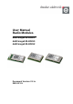
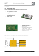


Table Of Contents
- 1. Overview
- 2. Applications
- 3. Features
- 4. Technical data
- 5. Mechanical size
- 6. Soldering profile
- 7. Pin assignment
- 8. PCB design
- 9. Clock
- 10. Application circuits
- 11. Programming
- 12. Pre-flashed firmware
- 13. Adapter boards
- 14. Radio certification
- 15. Ordering information
- 16. Packaging dimension
- 17. Revision notes
- 18. References

User Manual
Version 1.1c
2013-07-01
OEM radio modules deRFmega
www.dresden-elektronik.de
Page 2 of 52
Table of contents
1. Overview ......................................................................................................................... 6
2. Applications ..................................................................................................................... 6
3. Features .......................................................................................................................... 7
3.1. deRFmega128-22M00 ............................................................................................ 7
3.2. deRFmega128-22M10 ............................................................................................ 8
3.3. deRFmega128-22M12 ............................................................................................ 9
4. Technical data ............................................................................................................... 10
4.1. TX Power register settings for deRFmega128-22M00 and 22M10 ........................ 13
4.2. TX Power register settings for deRFmega128-22M12 .......................................... 14
4.3. Output power and duty cycle settings for deRFmega128-22M00 .......................... 15
4.4. Output power and duty cycle settings for deRFmega128-22M12 .......................... 16
5. Mechanical size ............................................................................................................. 17
5.1. deRFmega128-22M00 .......................................................................................... 17
5.2. deRFmega128-22M10 .......................................................................................... 18
5.3. deRFmega128-22M12 .......................................................................................... 19
6. Soldering profile............................................................................................................. 20
7. Pin assignment .............................................................................................................. 21
7.1. Signals of deRFmega128-22M00 ......................................................................... 21
7.2. Signals of deRFmega128-22M10 ......................................................................... 24
7.2.1. External front-end and antenna diversity control ....................................... 27
7.3. Signals of deRFmega128-22M12 ......................................................................... 28
7.3.1. Internal front-end control ........................................................................... 31
7.4. Signal description ................................................................................................. 32
8. PCB design ................................................................................................................... 34
8.1. Technology ........................................................................................................... 34
8.2. Base board footprint ............................................................................................. 34
8.2.1. Footprint of deRFmega128-22M00 ........................................................... 35
8.2.2. Footprint of deRFmega128-22M10 ........................................................... 36
8.2.3. Footprint of deRFmega128-22M12 ........................................................... 37
8.3. Ground plane........................................................................................................ 37
8.4. Layers .................................................................................................................. 38
8.5. Traces .................................................................................................................. 39
8.6. Placement on the PCB ......................................................................................... 40
9. Clock ............................................................................................................................. 41
10. Application circuits ......................................................................................................... 42
10.1. UART ................................................................................................................... 42
10.2. ISP ....................................................................................................................... 42
10.3. JTAG .................................................................................................................... 42
10.4. TWI ...................................................................................................................... 43
10.5. External front-end and antenna diversity .............................................................. 44
11. Programming ................................................................................................................. 46