
User's Manual
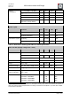
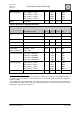

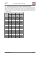


Table Of Contents
- 1. Overview
- 2. Applications
- 3. Features
- 4. Technical data
- 5. Mechanical size
- 6. Soldering profile
- 7. Pin assignment
- 8. PCB design
- 9. Clock
- 10. Application circuits
- 11. Programming
- 12. Pre-flashed firmware
- 13. Adapter boards
- 14. Radio certification
- 15. Ordering information
- 16. Packaging dimension
- 17. Revision notes
- 18. References

User Manual
Version 1.1c
2013-07-01
OEM radio modules deRFmega
www.dresden-elektronik.de
Page 12 of 52
Data rate (gross)
TRX_CTRL_2 = 0x00
TRX_CTRL_2 = 0x01
TRX_CTRL_2 = 0x02
TRX_CTRL_2 = 0x03
250
500
1000
2000
kBit/s
kBit/s
kBit/s
kBit/s
EVM
conducted
6.5
7.5
10.5
%
Table 4-6: Radio data of deRFmega128-22M12
Radio (Supply voltage VCC = 3.3V)
Parameter / feature
Min
Typ
Max
Unit
RF pad
Impedance
50
Ω
Diversity
Yes
Range
TBD
m
Frequency range
2405
2480
MHz
Channels
16
Transmitting
power conducted
2,3
TX_PWR = 0x00
VCC = 3.3V
21.4
21.9
22.4
dBm
Receiver sensitivity
Data Rate = 250 kBit/s
Data Rate = 500 kBit/s
Data Rate = 1000 kBit/s
Data Rate = 2000 kBit/s
-105
-100
-98
-91
dBm
dBm
dBm
dBm
Data rate (gross)
TRX_CTRL_2 = 0x00
TRX_CTRL_2 = 0x01
TRX_CTRL_2 = 0x02
TRX_CTRL_2 = 0x03
250
500
1000
2000
kBit/s
kBit/s
kBit/s
kBit/s
EVM
conducted
6.5
7.5
9.5
%
2
Only applicable for EU: The maximum allowed TX_PWR register setting of deRFmega128-22M12 is
TX_PWR = 0x0E. According to EN 300 328 clause 4.3.1 the maximum transmit power is restricted to
a limit of +10dBm.
3
Only applicable for US: Operating the transmitter at channel 11, 12, 13, 23, 24, 25 and 26 requires to
ensure a reduced output power and/or duty cycle limit to fulfil all requirements according to FCC Part
15 Subpart C § 15.209. See chapter 4.3.